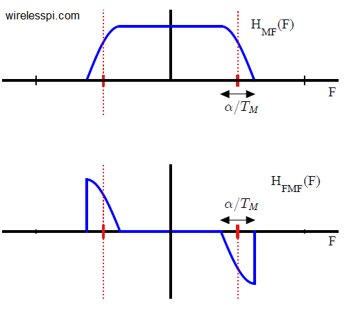
A matched filter in continuous frequency domain along with the corresponding frequency matched filter for excess bandwidth 0.25

Band Edge Filters for Carrier and Timing Synchronization

Band edge filters for carrier frequency and symbol timing synchronization is a very interesting topic that elegantly relates the tool (DSP) to the application (SDR design). This article is a short summary of where they originate from and what role they play for synchronization purpose. A Carrier Frequency Offset (CFO) arises due to a mismatch between Tx and Rx local oscillators as well as a phenomenon known as Doppler effect. In some other articles on this website, you will also find information on the Phase Locked Loop (PLL) in the context of carrier phase and timing synchronization. There is another

Continue reading
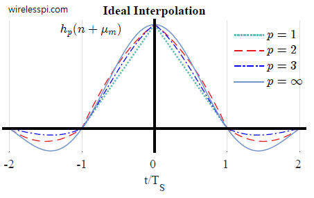
An increasing degree of polynomial approximation takes the filter closer and closer to an ideal sinc impulse response

Interpolation in Digital Communication Receivers

Timing synchronization in a digital receiver is about finding the right symbol peak and the symbol rate at which digital samples are taken for decisions purpose in a constellation diagram. In general, interpolation is the process of reproducing a missing sample at a desired location. In digital and wireless communications, the role of interpolation can be explained as follows. Background Imagine a Tx signal constructed from the upsampled and pulse shaped modulation symbols. The job of the Rx is to sample this waveform at optimal intervals, i.e., exactly at the middle of the eye diagram. In other words, the Rx

Continue reading
Block diagram of a pulse amplitude modulator and demodulator

Pulse Amplitude Modulation (PAM)

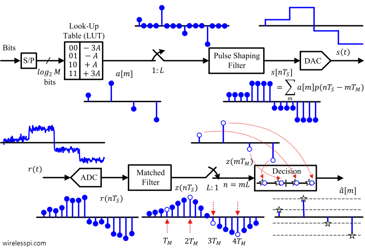
In the article on modulation – from numbers to signals, we said that the Pulse Amplitude Modulation (PAM) is an amplitude scaling of the pulse $p(nT_S)$ according to the symbol value. What happens when this process of scaling the pulse amplitude by symbols is repeated for every symbol during each interval $T_M$? Clearly, a series of bits $b$ (1010 in our initial example) can be transmitted by choosing a rectangular pulse and scaling it with appropriate symbols. \begin{equation*} \begin{aligned} m = 0 \quad b = 1 \quad a[0] = +A \\ m = 1 \quad b = 0 \quad a[1]

Continue reading
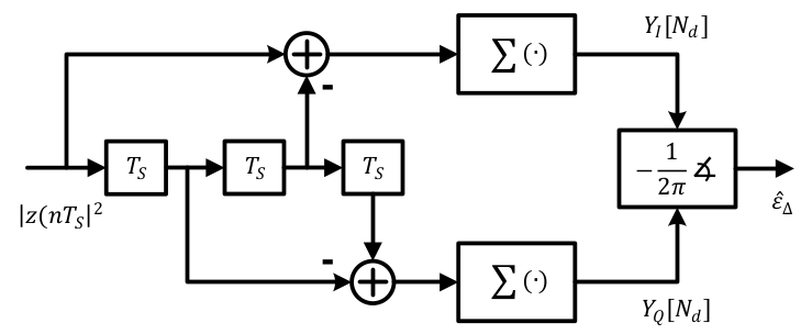
A block diagram for the implementation of a digital filter and square timing recovery for L=4 samples/symbol

Digital Filter and Square Timing Recovery

We have seen before how a symbol timing offset severely impacts the constellation of the received symbols. Therefore, symbol timing recovery is one of the most crucial jobs of a digital communications receiver. In the days of analog clock recovery, a timing error detector provided the instant to sample the Rx waveform at 1 sample/symbol at the maximum eye opening. However, discrete-time processing opened the doors for better timing recovery schemes as an ever increasing number of transistors within the same area consistently keeps bringing the digital processing cost down. Consequently, the use of analog circuits to control the timing

Continue reading