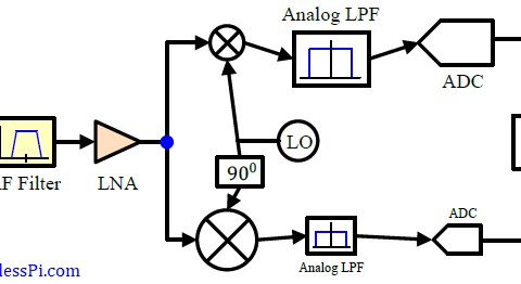
A Direct Digital Synthesizer (DDS) is an integral part of all modern communication systems. It is a technique to produce a desired waveform, usually a sinusoid, through employing digital signal processing algorithms. As an example, in the transmitter (Tx) of a digital communication system, a Local Oscillator (LO) is required to generate a carrier sinusoid that upconverts the modulated signal to its allocated frequency in the spectrum. On the receive (Rx) side, another local oscillator downconverts this high frequency signal to baseband for further processing. Such a process is shown in the Tx and Rx block diagrams of a Quadrature Amplitude Modulation (QAM) system below.

In addition to frequency translations, an oscillator with an adjustable frequency is also needed for synchronization purposes. While the above diagram shows an all-digital modem, the local oscillator can actually be implemented in both analog and digital domains. In most applications, however, discrete-time oscillators have widely replaced analog local oscillators in modulators and demodulators of modern communication systems.
A DDS is a discrete-time oscillator that consists of a Numerically Controlled Oscillator (NCO) followed by a Digital to Analog Converter (DAC) as shown below.

We start with an overview of advantages a DDS has over its analog counterpart.
Advantages
As we have seen before, there are several advantages a digital component offers over its analog counterpart.
- Implementation of digital signal processing techniques relies on computing platforms such as very large-scale integrated circuits that increasingly benefit from Moore’s law: the number of transistors in a dense integrated circuit (IC) doubled about every two years. This lead to gradual cost and performance advantages over the years. While its power consumption needs to be brought down further, a state-of-the-art DDS today such as Analog Devices AD9837 programmable waveform generator consumes 8.5 mW when operating at 2.3 V.
- Since digital switching can occur at extremely fast rates, switching between different frequencies at a fast rate becomes possible in a DDS (think of a frequency hopping system with a large spreading factor, for example). In addition, operation over a wide range of frequencies can be performed without much degradation in waveform quality.
- A DDS is capable of implementing arbitrary waveforms and direct digital modulations such as FSK and PSK.
- As we will find below, a fine frequency resolution can be obtained through selecting an appropriate clock rate and phase accumulator width.
Let us discuss the workings of the NCO in detail now. Keep in mind that the DDS output does not necessarily have to be a sinusoid. Practically any kind of waveform can be generated with a proper design.
Building an NCO
Denoting the instantaneous phase of a waveform as $\theta(t)$, the starting point is the relationship between frequency and phase defined as
\[
2\pi f = \frac{d\theta(t)}{dt},
\]
i.e., frequency is the rate of change of phase. The requirement of an adjustable frequency ‘on-the-fly’ and synchronizing the output with frequency and phase of an incoming waveform implies that the rate of change of phase need not be a constant.
\[
v(t) = \frac{d\theta(t)}{dt}
\]
Our target is to update the contents of a register, commonly called a Frequency Control Word (FCW), that automatically adjusts the instantaneous phase $\theta(t)$ at the output. This can be done by utilizing the above expression.
\[
\theta(t) = \int _{-\infty}^{t} v(\tau) d\tau
\]
where we have ignored the oscillator gain $k_0$. A digital version of the above integration can be written as
\[
\theta[n] = \sum _{i=-\infty}^{n-1} v[i]
\]
From the article on discrete-time integrators, we can deduce that this is a backward difference integrator.
\begin{align}
\theta[n] &= \sum _{i=-\infty}^{n-1} v[i] = \sum _{i=-\infty}^{n-2} v[i] + v[n-1] \nonumber \\
&= \theta[n-1] + v[n-1] ~~~\text{mod}~ 2\pi \label{equation-dds-backward-difference}
\end{align}
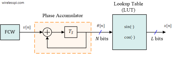
A block diagram for this NCO is drawn in the figure below. Here, the input $v[n]$ coming from the Frequency Control Word is summed into a register with its previous value that results in a running sum output. This forms the input to a Lookup Table (LUT) consisting of the samples of the discrete-time sinusoid (cosine, sine, or both). Sometimes this is also known as phase-to-amplitude conversion. The output is thus given as
\[
x[n] = \cos \left(\theta[n]\right) = \cos \left(\sum _{i=-\infty}^{n-1} v[n]\right)
\]
The NCO shown above is an idealized system. In practice, finite precision arithmetic generates spurs or unintended spectral lines around the clean spectrum of the desired signal.
Computing the Frequency Control Word (FCW)
There are two components of the NCO that are impacted by using finite precision arithmetic: phase accumulator and the cosine/sine Lookup Table. From the above diagram, observe that the number of samples stored in the Lookup Table is determined by the phase accumulator output because its contents form the address to the Lookup Table. The most common approach is to use 2’s complement arithmetic for phase accumulation so that the rollover from $+\pi$ to $-\pi$ is integrated automatically into the process.
In this regard, let $N$ represent the number of bits used to represent the contents of the phase accumulator. We track the following steps to compute the Frequency Control Word (FCW) for any particular frequency.
- A phase accumulator with content width of $N$ bits contains $2^{N}$ values.
- When FCW=1, the accumulator counts through every single sample of the Lookup Table, thus completing a full cycle of the maximum possible period (the lowest possible frequency), or frequency resolution $F_{res}$. This is drawn in the form of a phase wheel of equally-spaced angular values in the figure below. The Lookup Table outputs the corresponding sinusoid values.
- This counting happens at the clock rate or sample rate $F_{clock}$.
In light of the above, $F_{res}=1/T_{res}$ can be found by stepping through $2^{N}$ values at a rate of $F_{clock}=1/{T_{clock}}$ and hence we can write
\[
T_{res} = 2^N\times T_{clock}
\]
or
\[
F_{res} = \frac{F_{clock}}{2^{N}}
\]

We conclude that this frequency resolution is only set by the clock or sample rate and the accumulator size. For example, the Analog Devices AD9837 mentioned earlier has $N=28$ with $16$ and $5$ MHz clock rates. This implies that it can achieve the following frequency resolutions.
\[
\begin{aligned}
F_{res} &= \frac{16\times 10^6}{2^{28}} \approx 0.06~\text{Hz}\\
F_{res} &= \frac{5\times 10^6}{2^{28}} \approx 0.02~\text{Hz}
\end{aligned}
\]
Moving forward, when FCW=2 as shown in the figure above, the phase accumulator steps through every second value, thus producing a waveform with frequency $2F_{res}$ and so on. This allows us to write for a general desired frequency $F_0$,
\[
F_0 = FCW\times F_{res} = FCW\times \frac{F_{clock}}{2^{N}}
\]
From here, the expression for FCW for any frequency $F_0$ can be found as
FCW = \frac{F_0\cdot 2^N}{F_{clock}}
\]
where $N$ is the accumulator width and $F_{clock}$ is the sample rate. A change in FCW appears at the output instantaneously, as opposed to a Phase-Locked Loop (PLL) that requires a certain settling time.
For a 500 MHz clock and a 32-bit phase accumulator, the resolution is given by
\[
F_{res} = \frac{500\times 10^6}{2^{32}} \approx 0.12~\text{Hz}
\]
For an output frequency of $F_0=48$ MHz, the FCW should be
\[
FCW = \frac{(48\times 10^6)(2^{32})}{500\times 10^6} \approx 412316860
\]
From the sampling theorem, the maximum frequency can also be determined as $F_m = F_{clock}/2$. These expressions can also be used backwards, e.g., to determine the accumulator width for a given frequency resolution and clock rate.
Next, we look into techniques to reduce the size of the Lookup Table.
Lookup Table Reduction
Notice that for a phase accumulator width of $N=32$ bits, there will be 32 address lines probing the Lookup Table that would have a number of entries given by
\[
2^{32} = 4,294,967,296 > 4~\text{billion}
\]
If each such entry is represented by $L=16$ bits, we need
\[
2^{32}\times 16 = 68.72~\text{Gbits}
\]
We think of memory sizes in Gigabits as normal but this is a considerably large size for a small component of a simple waveform generator and becomes infeasible for high speed operations in particular. Two straightforward methods through which its size can be reduced are described next.
Quarter Cycle Storage
The simplest approach is to exploit the inherent symmetries in sine and cosine waves given by fundamental trigonometric relations. For example, for a sine wave, we have
\[
\begin{aligned}
\sin \theta &= -\sin (-\theta) \qquad \qquad -\pi \le \theta \le \pi \\
\\
\sin \left(\frac{\pi}{2}-\theta\right) &= \sin \left( \frac{\pi}{2}+\theta\right) \qquad \qquad 0 \le \theta \le \frac{\pi}{2}
\end{aligned}
\]
This is illustrated in the figure below.

From an algorithmic perspective, if only a sine wave is stored, this turns out to be count up, count down, count up with negative sign and count down with negative sign. On the other hand, we have for a cosine,
\[
\begin{aligned}
\cos \theta &= \cos (-\theta) \qquad \qquad\qquad -\pi \le \theta \le \pi \\
\\
\cos \left(\frac{\pi}{2}-\theta\right) &= -\cos \left( \frac{\pi}{2}+\theta\right) \qquad \qquad 0 \le \theta \le \frac{\pi}{2}
\end{aligned}
\]
From an algorithmic perspective, if only a sine wave is stored, this turns out to be count down, count up with negative sign, count down with negative sign and count up. In this way, the values of the sine wave in one quarter cycle can be used to determine the values in the remaining three quarter cycles for both inphase and quadrature parts.
Truncating the Phase Accumulator
As mentioned earlier, the phase accumulator output $\theta[n]$ is $N$ bits wide where $N$ is a large number. Here, a certain number, say $w$, of Least Significant Bits (LSBs) at the output of the phase accumulator are truncated to reduce the word width for $\hat \theta [n]$ to $N-w=B$ bits. Then, these $B$ address lines are input to the Lookup Table which now has a reduced size of $2^B$ entries. Keep in mind that any number of bits, e.g., $L=32$, can still be used for representing each such entry. This is drawn in the block diagram below.

The price to pay for this now smaller Lookup Table is phase noise in the generated waveform. For a sinusoidal wave, this can be seen as additional spectral lines in the output spectrum, although a sinusoid spectrum should contain only a single impulse.
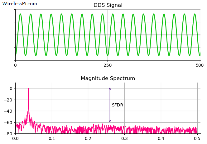
Let us take an example of a complex sinusoid with normalized frequency $0.036$ cycles/sample generated by a DDS for the following parameters.
\[
N = 24, \quad B = 8, \quad L = 16
\]
Here, the phase accumulator has a width of $N=24$ bits which is truncated to $B=8$ bits. This results in a small Lookup Table of size $2^8=256$, each element of which has $L=16$ bits of precision.
Since the spectrum of a complex sinusoid is a single impulse, the Discrete Fourier Transform (DFT) of the waveform should be zero at all the other frequencies. However, when the DFT of such a waveform is taken, we see spectral energy appearing at other bins due to the quantization of phase accumulator output. These lines are known as spurs.

Clearly, the quality of the waveform is affected by the largest spur. Therefore, the difference between the desired waveform magnitude and the largest spur magnitude is known as Spurious-Free Dynamic Range (SFDR), which plays an important role in signal analysis in addition to the Signal to Noise and Distortion Ratio (SINAD).
Next, we discuss the origin of these spectral lines and then describe techniques to reduce their magnitude.
Spurious Spectral Lines
Recall that the phase accumulator output is truncated to reduce the Lookup Table size. This introduces a phase error equal to
\[
\Delta _\theta[n] = \theta[n] ~-~ \hat \theta [n]
\]
If the desired waveform is a complex sinusoid, it can now be written as
\begin{equation}\label{equation-dds-phase-error}
e^{j\theta[n]} = e^{j\hat \theta[n]}\cdot e^{j\Delta _\theta[n]}
\end{equation}
The shape of $\Delta _\theta[n]$ is determined by the target waveform. For a complex sinusoid in which phase keeps increasing at a constant rate, this phase error is a ramp function that becomes a sawtooth wave after the periodic rollover. The DFT of such a signal has Fourier coefficients at all harmonics. These harmonics appear as spurs in the waveform spectrum at locations that are determined by
- the Lookup Table size $2^B$, and
- the phase increment as a function of $2^N$.
As an example, in the above figure, the largest spurious line appears at a normalized frequency of approximately $0.25$ cycles/sample where its magnitude is seen as $-48$ dB. Comparing with a 0 dB signal magnitude, the SFDR is computed as $0-(-48)=48$ dB.
We now discuss the techniques to reduce the magnitude of these spectral lines for low phase noise at the output.
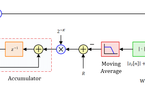
Feedforward Error Removal
Notice from Eq (\ref{equation-dds-phase-error}) that both the phase accumulator output $\theta[n]$ and its truncated version $\hat \theta[n]$ are known quantities. This implies that the resulting phase error $\Delta_\theta[n]$ can be computed and then utilized to compensate for the error in the Lookup Table output. When this phase error is small, Euler’s identity as well as sine and cosine approximations can be employed to simplify the procedure, i.e., for a small $\theta$, $\cos \theta \approx 1$ and $\sin \theta \approx \theta$.
\[
\begin{aligned}
e^{j\theta[n]} &= e^{j\hat \theta[n]}\cdot e^{j\Delta _\theta[n]} \\
&= e^{j\hat \theta[n]}\left\{\cos(\Delta _\theta[n]) + j\sin (\Delta _\theta[n]) \right\}\\
&\approx e^{j\hat \theta[n]}\left(1 + j\Delta _\theta[n]\right)
\end{aligned}
\]
This is drawn in the block diagram below in the form of a complex multiplication. The actual real multiplications can be derived by using Euler’s identity to open $e^{j\hat \theta[n]}$ in the last equation above.

While this technique produces excellent results, the main disadvantage is the computational complexity. Two multiplications and two additions are required to generate each output sample. This becomes a bottleneck in performance for large sample rates.
As opposed to error feedforward method, a feedback error removal technique is also feasible in which the phase error is estimated and removed prior to truncation. This error prediction is performed by employing a Finite Impulse Response (FIR) filter, known as a linear predictor in this context. This also results in noise shaping where the noise power is mostly suppressed in the neighborhood of the desired signal but significantly higher at frequencies away from it.
Dithering
The root cause of spurious spectral lines is the periodic structure of the phase ramp $\Delta_\theta[n]$. A periodic signal has its Fourier Series coefficients at certain discrete frequencies that tend to be much larger than other random frequency components. On the other hand, the spectrum of a random signal, say noise, is distributed across the entire range.
The solution then lies in breaking this periodic pattern through addition of a random signal. Dithering is a technique that accomplishes this task by adding a small amount of random noise to the phase accumulator output before its truncation. A block diagram of such a procedure is drawn in the figure below.

Let us dither the phase accumulator output in a DDS implementation with the same parameters as in the example described before, i.e., phase accumulator width $N = 24$, truncated output with $B = 8$ bits and a Lookup Table with $L = 16$ bits of precision. The resulting waveform along with its spectrum is plotted in the figure below with the following observations.
- The DDS noise floor is spread across the entire range because the random noise has a distributed spectrum.
- There are no visible discrete spectral lines since the noise has disrupted the periodic structure in the phase error.

Looking at the noise floor, we can see that the Spurious-Free Dynamic Range is now 60 dB. As compared to the regular DDS discussed in the example before where this value was found to be 48 dB, dithering has improved the SFDR by 12 dB. Recalling the familiar rule of 6 dB per bit, this technique has resulted in an improvement worth 2 bits of precision. In other words, the DDS output with $B=8$ bits and dithering is equivalent to a regular DDS output with $B=10$ bits and no dithering!
Dithering is also used in image processing applications, see an example here.
Direct Digital Modulation
For an efficient implementation, a DDS supports direct digital modulation as well such as Frequency Shift Keying (FSK), Phase Shift Keying (PSK) and Amplitude Shift Keying (ASK). For this purpose, we are already familiar with the Frequency Control Word (FCW) that defines the frequency of the output waveform. In a similar manner, a Phase Control Word (PCW) and an Amplitude Control Word (ACW) can be introduced at suitable places to directly control the phase and amplitude, respectively, of the output waveform. A block diagram of such an implementation is illustrated below.

This has proved to be an attractive feature of the DDS for low power communication modules.
Really nice and concise article, Kudos. A naive question: so where is the PLL in all this? Is it placed in clock for sampling the ADC?
See these articles on carrier PLL and timing PLL for an explanation.