We have discussed before the sampling on time axis for analog to digital (A/D) conversion. An Analog to Digital Converter (ADC) produces the samples $x[n]$ of a continuous-time signal $x(t)$ at its input. Ideally, these samples are the exact values of the signal $x(t)$ at time instants $nT_s$ where $T_s=1/f_s$ is the sampling period. In practice, however, there are imperfections both on the y-axis and the x-axis.
- On y-axis, an ADC has a finite resolution depending on the number of bits used for quantization.
- On x-axis, there are issues of clock jitter that distort the samples produced.
In this article, I explain why the Signal to Noise Ratio (SNR) at the ADC output improves by 6 dB for each extra bit of resolution and address the topics of oversampling and undersampling. My attempt is to unify the multitude of expressions and values in ADC datasheets and help clarify any confusions in this regard.
Quantization Error
Most of the world produces analog signals and Analog-to-Digital Converters (ADCs) in our electronic products convert them into digital signals. On the y-axis, this is done by rounding off the samples to the closest quantized level at regular intervals as drawn in the figure below. These quantized levels are assigned binary representations according to the number of bits available for this conversion (e.g., the figure below illustrates 4 bits and $2^4=16$ corresponding levels in a range of $+V_{\text{max}}$ and $-V_{\text{max}}$).

In a way, this is similar to how a human mind works. Reality is infinitely complex in detail but we can only capture its quantized version through the ideas dictated by our language. This is why you will find all great thinkers adding different terms and expressions into their languages, thus pushing the boundaries and broadening the horizon of thought.
Coming back, observe that there is an error introduced on the amplitude axis during this process. This error is given by
\[
e[n] = x(nT_s) – x_q(nT_s)
\]
where $x_q(nT_s)$ is the waveform mapped on discrete levels above. This is drawn in the figure below.

We observe the following.
- The quantization error $e[n]$ is uniformly distributed between $+\Delta/2$ to $-\Delta/2$.
\[
\frac{\Delta}{2} ~<~ e[n] ~<~ +\frac{\Delta}{2} \] Its probability distribution function between these two values is given by \[ p(e) = \frac{1}{\Delta} \] Keep in mind that we are talking about quantization noise here, and not the Gaussian noise. Quantization noise is assumed as a white noise process that implies having the same power at all frequencies. Furthermore, it is uncorrelated with the input signal itself. A representative digital output vs analog input for an ideal ADC is shown in the figure below.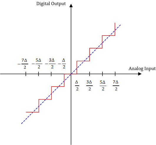
- The average value of the error turns out to be zero. This can be seen as
\[
\text{Avg}\left\{e[n]\right\} = \int _{-\frac{\Delta}{2}}^{+\frac{\Delta}{2}} e\cdot \frac{1}{\Delta} de = \frac{e^2}{2\Delta}\Bigg|_{-\frac{\Delta}{2}}^{+\frac{\Delta}{2}} = 0
\] - The power in the error signal is the same as its variance.
\begin{equation}
\begin{aligned}
\sigma_e^2 &= \int _{-\frac{\Delta}{2}}^{+\frac{\Delta}{2}} e^2\cdot \frac{1}{\Delta} de = \frac{e^3}{3\Delta}\Bigg|_{-\frac{\Delta}{2}}^{+\frac{\Delta}{2}} \\\\
&= \frac{1}{3\Delta}\left[ \frac{\Delta^3}{8} + \frac{\Delta^3}{8}\right] \\\\
&= \frac{\Delta^2}{12}\label{equation-noise-power}
\end{aligned}
\end{equation}Consequently, the Root Mean Square (RMS) value of the quantization noise is given by
\begin{equation}\label{equation-rms-noise}
\sigma_e = \frac{\Delta}{\sqrt{12}}
\end{equation}With noise power in hand, we can now turn towards deriving the RMS value for a sinusoidal signal.
A Sinusoidal Input
To find the SNR, we need the RMS value of a sinusoid that acts as the reference signal. A sinusoidal signal is important because almost all signals are made up of sinusoids. For a peak value of $A$ and frequency $\omega$, we can compute this value over a period $T$ as follows.
\[
\begin{aligned}
\sigma_x &= \sqrt{\frac{1}{T}\int_{0}^{T}A^2 \cos^2 (\omega t) dt} \\ \\
&= \sqrt{\frac{A^2}{T}\int_{0}^{T} \frac{1+\cos (2\omega t)}{2} dt} \\ \\
&= \sqrt{\frac{A^2}{2T}t\bigg|_{0}^{T} + \underbrace{\frac{A^2}{2T}\int_{0}^{T}\cos (2\omega t) dt}_{0}}
\end{aligned}
\]where we have used the fact that the area under the curve for one cycle of a sinusoid is zero due to both positive and negative halves spanning a complete period. The RMS value is thus
\begin{equation}\label{equation-rms-sinusoid}
\sigma_x = \frac{A}{\sqrt{2}}
\end{equation}Now we can derive the quantization SNR as below.
Signal to Quantization Noise Ratio
Under the assumption that the error signal is uncorrelated with the signal samples, the signal to quantization noise ratio can be determined as follows.
\[
\text{SNR} = \frac{\sigma_x}{\sigma_e}
\]From Eq (\ref{equation-rms-sinusoid}) and Eq (\ref{equation-rms-noise}), we have
\[
\text{SNR} = 20\log_{10} \left[\frac{A}{\sqrt{2}}\cdot \frac{\sqrt{12}}{\Delta}\right]
\]As shown in the top figure above, if the top and bottom scales of the ADC are given by $+V_{\text{max}}$ and $-V_{\text{max}}$, respectively, and there are $N$ bits of precision, then there are $2^N$ steps in a range of $2V_{\text{max}}$ as
\[
\Delta = \frac{2V_{\text{max}}}{2^N}
\]Plugging in the value for $\Delta$ in the SNR expression, we get
\begin{equation}\label{equation-general-snr}
\text{SNR} = 20\log_{10} \left[\frac{A}{\sqrt{2}}\cdot \frac{\sqrt{12}}{2V_{\text{max}}} \cdot 2^N\right]
\end{equation}Computing the logarithms yields the final expression.
\begin{equation}\label{equation-snr}
\text{SNR} = 6.02 N + 1.76 ~-~ 20\log_{10} \frac{V_{\text{max}}}{A} \quad \text{dB}
\end{equation}Let us describe what we can infer from the above equation.
6 dB per Bit SNR
It is clear from the above equation why each extra bit contributes an SNR improvement of around 6 dB. This extra bit doubles the number of quantization levels (e.g., going from $2^{14}$ levels in a 14-bit ADC to $2\times 2^{14}$ in a 15-bit ADC).
Role of Full-Scale Amplitude
The last term in Eq (\ref{equation-snr}) is the ratio of full-scale ADC amplitude $V_{\text{max}}$ with the peak amplitude of the waveform $A$. A minus sign indicates the performance penalty in the ADC SNR by not operating at the full scale. If $A=V_{\text{max}}$, this ratio is 1 and the logarithm is zero, thus yielding the well-known expression
\[
\text{SNR} = 6.02 N + 1.76 \quad \text{dB}
\]The number of bits $N$ can be computed from the above equation. In practice, not only noise but harmonics also distort the input signal for which Signal to Noise and Distortion ratio SINAD is a better metric. Therefore, Effective Number of Bits (ENOB) is found by replacing SNR by SINAD in the above equation as
\[
\text{ENOB} = \frac{\text{SINAD} – 1.76}{6.02}
\]Coming back to the SNR expression above, it seems that when $A > V_{\text{max}}$, the ratio $V_{\text{max}}/A$ is less than 1 that should contribute a positive term to the SNR. Nevertheless, when the signal amplitude goes beyond the ADC range, it results in clipping of the signal. Since clipping is a non-linear operation, severe distortion occurs with more spectral components at the output than present in the input signal $x(t)$. Instead, the operating point should be kept as close to 1 as possible. In a digital receiver, an Automatic Gain Control (AGC) keeps the input signal level to a set point (below the full scale) in an adaptive manner.
Peak to Average Ratio (PAR)
In deriving Eq (\ref{equation-snr}), we assumed a sinusoidal input that has a Peak to Average Ratio (PAR) of 3 dB due to the factor $1/\sqrt{2}$, see Eq (\ref{equation-rms-sinusoid}). What is the generalized expression as compared to the sinusoid with a $3$ dB PAR earlier?
For a general input with RMS value $\sigma_x$, we can modify Eq (\ref{equation-general-snr}) as
\[
\text{SNR} = 20\log_{10}\left[ \sigma_x \cdot \frac{\sqrt{12}}{2V_{\text{max}}} \cdot 2^N\right]
\]Since $20\log_{10}(\sqrt{12}/2)\approx 4.76$, we get
\[
\text{SNR} = 6.02 N + 4.76 ~-~ 20\log_{10} \frac{V_{\text{max}}}{\sigma_x} \quad \text{dB}
\]Multiplying and dividing the ratio in the last term by $A$,
\begin{equation}\label{equation-rms-par}
\text{SNR} = 6.02 N + \underbrace{4.76 ~-~ \underbrace{20\log_{10} \frac{A}{\sigma_x}}_{3 ~\text{dB}}}_{\text{Original}~1.76~\text{factor}} ~-~ 20\log_{10} \frac{V_{\text{max}}}{A}\quad \text{dB}
\end{equation}where $A/\sigma_x$ is taken from Eq (\ref{equation-rms-sinusoid}), the PAR for a sinusoidal signal. It is observed that in addition to the full-scale amplitude to peak value, the peak to average ratio is also important in determining the ADC performance.
The parameter PAR is a characteristic of the signal itself and not much can be done at the ADC side in this regard. It is desirable to have an input signal with low PAR to maximize the SNR at the ADC output. While sinusoidal signals have a 3 dB PAR, many digitally modulated signals have larger range. This problem is particularly severe for OFDM signals that suffer in the form of inefficiency from high PAR. A backoff is therefore required to prevent non-linear distortion from clipping. In ADC terminology, this is known as dBFS (i.e., dB below full scale).
Combining all three parameters, namely full-scale amplitude $V_{\text{max}}$, peak input amplitude $A$ and average signal power $\sigma_x$, in one place, we see their relationship in the figure below.
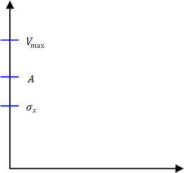
In summary, for better SNR, the target is to have $\sigma_x$ as close to $A$ as possible for a small peak to average ratio. In addition, the peak input amplitude $A$ should be close to full-scale amplitude $V_{\text{max}}$ but not too close to avoid clipping.
Oversampling
The discussion so far assumed a full bandwidth signal due to which the noise power was considered in the whole range of the first Nyquist zone, $-f_s/2$ to $+f_s/2$ where $f_s$ is the sample rate. The SNR at the ADC output can be increased by oversampling the signal.
In time domain, it is obvious that the more closely the samples are spaced apart, the better the approximation leading to a reduction in quantization noise.
A frequency domain view is more interesting as shown in the figure below.
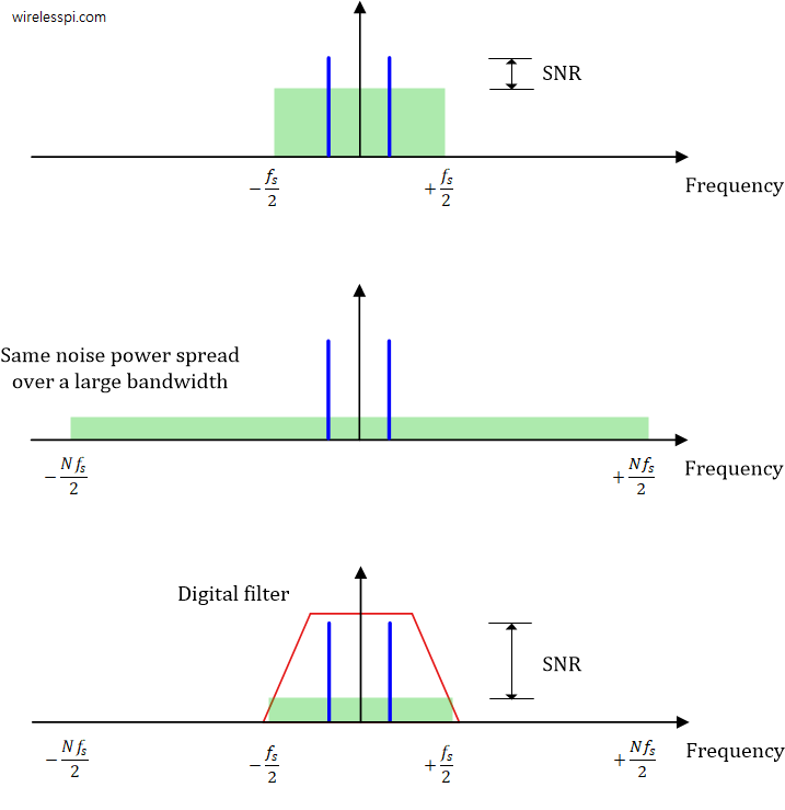
Let us trace the following line of reasoning from this spectral perspective.
- The top figure plots a regular ADC sampling a signal at a rate of $f_s=B$. The SNR is marked as the ratio between the signal power (a real sinusoid with a spectrum of two impulses) and the quantization noise power. All the power is constrained within the bandwidth $B$, or $-f_s/2$ to $+f_s/2$.
- In the second figure, an oversampling ADC samples at a rate $N$ times higher due to which the same noise power is now spread between $-Nf_s/2$ to $+Nf_s/2$. Since power is area under the curve, a wide bandwidth implies a reduction in height of this density. However, we have not gained any benefit from oversampling yet.
- A digital filter rejects the spectral contents outside the initial bandwidth $B$ or $+f_s/2$. This operation discards the noise power outside this range as well. As a consequence, there is a $\sqrt{N}$ times improvement in SNR within the signal bandwidth after this filtering (for the same power, the spectral density is scaled by $1/\sqrt{N}$ with the new sample rate).
With $N$ being the oversampling factor, this brings us to the final equation that determines the SNR at the output.
\[
\text{SNR} = 6.02 N + 4.76 ~-~ 20\log_{10} \frac{A}{\sigma_x} ~-~ 20\log_{10} \frac{V_{\text{max}}}{A} ~+~ 10\log_{10}N\quad \text{dB}
\]From the above equation, we can see why the oversampling factor is also known as the processing gain. In words, this equation can be expressed as
\[
\begin{align*}
\text{SNR} &= 6.02 N + 4.76 ~-~ \text{Peak to average ratio} ~-~ \\ &\\ &\qquad\text{Full-scale amplitude to peak ratio} ~+~ \text{Oversampling factor (dB)}
\end{align*}
\]Finally, let us turn our attention towards the idea of undersampling a bandpass signal.
Undersampling a Bandpass Signal
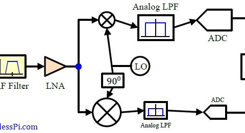
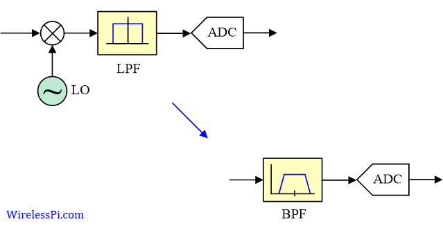
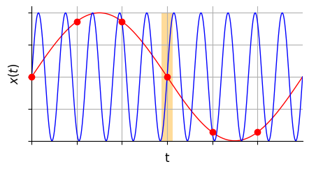
We learned in the process of sampling a signal that aliases are produced at integer multiples of the sample rate $f_s$. We can deduce that instead of downconverting a signal through a Local Oscillator (LO) and filter before the ADC, we can directly sample the bandpass signal and filter the required alias at baseband through digital processing. This is drawn in the figure below.

In theory, a frequency domain view entails several signal spectra of the signal at integer multiples of sample rate, one of which can be captured through an appropriate bandpass filter. This is because a continuous frequency higher than $f_s/2$ Hz appears similar to a frequency $f_s$ Hz apart from itself as plotted in the figure below. Observe that samples are taken at a rate such that both sinusoids pass through the same points. In fact, there are infinitely many sinusoids ($f_s$ Hz apart) which pass through the same points, and hence become indistinguishable from each other after sampling.
In practice, however, there are challenges that need to be overcome before bandpass sampling can be applied to digitize a signal. One such challenge is the sampling clock jitter that comes from small variations of the ideal instant around a mean value. As seen from the shaded rectangle in the above figure, there is a large amplitude error in the high frequency signal than the low frequency one for the same timing error. The exact expression for how this jitter impacts the amplitude of the sampled waveform can be derived as follows.
Again, consider a sinusoidal wave sampled at an instant $t=nT_s + \delta$ instead of the ideal time $t=nT_s$. The error between the two amplitudes is given by
\[
\Delta_A = A \cos (\omega nT_s) – A \cos \left[\omega (nT_s+\delta)\right]
\]Using the identity $\cos (\alpha+\beta)$ $=$ $\cos \alpha \cos \beta – \sin \alpha \sin \beta$, we get
\[
\Delta_A = A \cos (\omega nT_s) – A \left[\cos (\omega nT_s)\cos (\omega \delta) – \sin (\omega nT_s) \sin (\omega \delta)\right]
\]Since $\omega \delta$ is small, we can apply the small angle approximations.
\[
\cos\theta \approx 1 \quad\text{and}\quad \sin\theta \approx \theta \qquad \text{for small}~~ \theta
\]As a consequence, the amplitude error becomes
\[
\Delta_A = A\omega \delta \sin (\omega nT_s)
\]Since $|\sin (\omega nT_s)|$ is bounded by 1, we have
\[
|\Delta_A| < A\omega \delta \] As predicted, the loss in amplitude comes from three factors:- waveform amplitude $A$
- frequency of operation $\omega$
- clock jitter $\delta$
In conclusion, a factor proportional to $20\log_{10}(\omega \delta)$ is included with the quantization noise to further degrade the effective number of bits in an ADC. Furthermore, phase noise of the sampling clock also plays a major role in determining the ADC SNR for bandpass sampling that is dependent on the waveform and the frequency of interest.