"The fundamental problem of communication is that of reproducing at one point either exactly or approximately a message selected at another point."
Our main purpose is to transfer digital information – which is a sequence of bits 0’s and 1’s – from one system to another through a communication channel. Let us return for a moment to the concept behind simple digital logic where logic 0 can be assigned to one voltage level while logic 1 to another. Provided the static discipline is followed, all our system electronics has to do is to be able to differentiate between these two levels.
Of course, digital circuits also have real voltages and real currents which are never exact. The infinite voltage levels are just broken into two discrete regions. Hence, they remain close to that state when the real world noise is introduced, which makes the digital circuits very robust and noise tolerant. This breaking down of real numbers on a continuous scale into discrete regions is the basis of the whole digital revolution.
This particular philosophy is very close to human nature too. Think about it: we like to classify everyday stuff into clearly defined boxes. For example, day and night, black and white, good and bad. The reality, however, is continuous in the sense that the brightness of light varies throughout the 24 hours, there are multiple shades of grey, and people are much more complex than being simply good and bad.
Digital communication follows the same principle but allows for multiple discrete regions. Since many resources on digital communications concentrate on mathematical derivations of the concepts, we explain these concepts from more of an intuitive viewpoint without rigorous proofs.
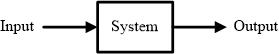
In wireless communications and other applications of digital signal processing, we often want to modify a generated or acquired signal. A device or algorithm that performs some prescribed operations on an input signal to generate an output signal is called a system.
In every digital communication system, whether it is a home DSL or cellular data plan, one fundamental parameter we always hear about is the data rate. Data rate is simply the number of bits transmitted and received during one second, also called the bit rate denoted by $R_b$ bits/second (b/s). Stated in another way, the source produces one bit during every $1/R_b = T_b$ seconds.
Since these bits consist of 0’s and 1’s, we start with assigning them two distinguishable voltage levels $-A$ and $+A$, an example of which is shown in the figure below. Such a representation is called a constellation. Our ultimate purpose is to transmit a sequence of these voltage levels according to the bit stream at the Tx side. Then, we design the system such that these voltage levels are received undistorted in every manner at the Rx side so that the Rx can perform the inverse mapping from voltage to bits and find out the original bit stream.
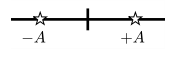
Based on this reasoning, a very simple digital communication system can be built as follows: At the Tx side, logic 0 and 1 of a bit sequence $\underline{b}$ are mapped to levels $-A$ and $+A$ of a symbol sequence $a[m]$, respectively, at discrete time intervals $m = 0,1,2,\cdot\cdot\cdot$. This process is called bit-symbol mapping and the time index $m$ counts each such symbol time, $T_M$. A symbol is basically a mapping from the binary logic levels to signal levels into the real world. The constellation in the figure above illustrates the relationship between bits in $\underline{b}$ and symbols $a[m]$ as
\begin{equation}
a[m] = \left\{ \begin{array}{l}
-A, \quad b = 0 \\
+A, \quad b = 1 \\
\end{array} \right.
\end{equation}
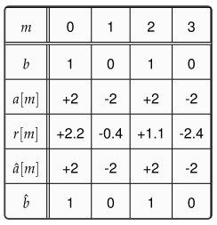
For a bit sequence 1010, the generated symbols for $A=2$ are shown in Table below.
The block diagram of such a system is shown in the figure below. The received signal is corrupted by the addition of random noise $w[m]$ on the Rx side such that the the received signal $r[m]$ is given as
\begin{equation*}
r[m] = a[m] + w[m]
\end{equation*}
As a consequence of noise addition, the received symbols are scattered around the actual symbol values as illustrated in the decision block of the figure above. Common sense dictates that symbol decisions $\hat a[m]$ should be taken according to the following rule:

If $r[m]$ is closer to $-A$, it is decided that symbol $-A$ was sent at time $m$, and if it closer to $+A$, it is taken as symbol $+A$. To construct a general intuitive rule, the point in their middle is $(-A+A)/2=0$, and hence
\begin{equation}\label{eqCommSystemBinaryDecisionRule}
\hat a[m] = \left\{ \begin{array}{l}
-A, \quad r[m] < 0 \\
+A, \quad r[m] > 0 \\
\end{array} \right.
\end{equation}
Such a decision rule is applied to compute $\hat a[m]$ in Table above for $A=2$ where we luckily encounter no errors. The above relation is actually a manifestation of the minimum distance rule. What is not evident here, and we find out in another article, is that we are actually performing a correlation with the two possible options and choosing the more likely one. Since we quoted Sherlock Holmes to introduce correlation, we recall another of his quote in this context:
"… we balance probabilities and choose the most likely.."
Finally, the subsequent symbol-bit mapping generates bit 0 for symbol $-A$ and bit 1 for symbol $+A$ to form the estimated bit sequence $\hat{b}$. Notice that the digital communication system constructed above is sending and receiving one bit in every symbol time $T_M$.