It is a little unusual to describe a hardware radio on a website that focuses on software radios. But I was impressed with the functionality and performance of AT86RF215 transceivers by Microchip during my experiments. I have used them for node localization and they can be put to many other good uses, including, …. here is the surprise, …. as software defined radios.
Through a little programming effort, I/Q samples from the digital frontend can be directly accessed using which you can run your own baseband on a digital signal processor. Although interfacing with an external device for I/Q samples delivery is not straightforward, this is a very powerful feature, among others, that this device has to offer.
If you like experimentation with radios and DSP, then this might be an option with the following pros and cons.
- Signal conditioning and processing in analog and digital domains is of professional grade, as opposed to most of the hardware and software employed in general software defined radios.
- You will not run into different kinds of widespread latency issues.
- As mentioned before, capturing the I/Q samples from the device is not straightforward. It is done through a 13-bit I/Q Low Voltage Differential Signal (LVDS) interface that can route the I/Q data directly to any external processor for application of DSP techniques. See the datasheet for the detailed procedure.
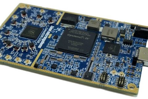
Below is the first look of the associated ATREB-XPRO evaluation board with the chip in the center.

Let us go into more technical details.
Introduction
The AT86RF215 is a multi-band radio transceiver for various sub-1GHz bands and the 2.4GHz band that is compliant to IEEE 802.15.4-2011, IEEE 802.15.4g-2012, and ETSI TS 102 887-1.standards. The applications include smart metering, smart lighting, home energy gateways, and other industrial and automation Internet of Things (IoT).
It supports the following multi-rate and multi-regional modulation schemes at the physical layer.
- MR-FSK
- Symbol rates: 50, 100, 150, 200, 300, 400 ksymbol/s
- Rate 1/2-FEC: RSC and NRNSC, with and without interleaving
- MR-OFDM
- Option 1: 100, 200, 400, 800, 1200, 1600, 2400 kb/s
- Option 2: 50, 100, 200, 400, 600, 800, 1200 kb/s
- Option 3: 50, 100, 200, 300, 400, 600 kb/s
- Option 4: 50, 100, 150, 200, 300 kb/s
- MR-OQPSK
- 100kchip/s with 6.25, 12.5, 25, 50 kb/s
- 200kchip/s with 12.5, 25*, 50, 100 kb/s
- 1000kchip/s with 31.25, 125, 250, 500 kb/s
- 2000kchip/s with 31.25, 125, 250, 500, 1000 kb/s
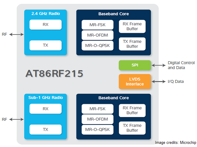
Both transceivers, in sub-GHz and 2.4 GHz bands, can operate simultaneously as each of them contains its own I/Q data interface and baseband engine, thus forming two independent radio systems. The figure below shows the block diagram of the chip (image courtesy of Microchip).

From a DSP perspective, the following features of Microchip AT86RF215 are particularly interesting.
Tx Frontend
Analog
As far as the Tx analog frontend is concerned, the transmitter is based on a direct upconversion architecture. After the digital to analog converter (DAC) the IQ signals are passed through an analog 2nd order low-pass filters which covers a cut-off frequency range from 80 kHz to 1000 kHz with uniform logarithmic stepping.

Digital
According to the datasheet, the Transmitter Digital Frontend (TX_DFE) performs discrete time sample rate conversion of the complex baseband signal based on a zero-Intermediate Frequency (zero-IF) architecture. The I/Q data sampling frequency $f_s$ is configured according to the relation
\[
f_s = \frac{4}{SR}~ \text{MHz}
\]
where SR is defined by a register named as TXDFE.SR. The signal processing flow is depicted in the figure below. The block PRE_FLT filters the baseband signal at the sampling frequency $f_s$.
To relax the interpolation complexity of the baseband processor that suppresses the unwanted images, a selection of suitable normalized cut-off frequencies $f_{\text{cut}}$ (TXDFE.RCUT) is available. For $f_{cut}$ equal to 1, this block is bypassed, reducing the group delay and latency. Upsampling from $f_s$ to 4MHz is accomplished by the block UP_SRC(1:SR) that employs a linear phase FIR interpolation filter with normalized cut-off frequency 1/SR. Finally, the block UP_SRC(1:8) upsamples to the DAC sampling frequency of 32MHz by employing three stages of linear phase FIR filters with normalized cut-off frequency $1/2$.
Rx Frontend
Analog
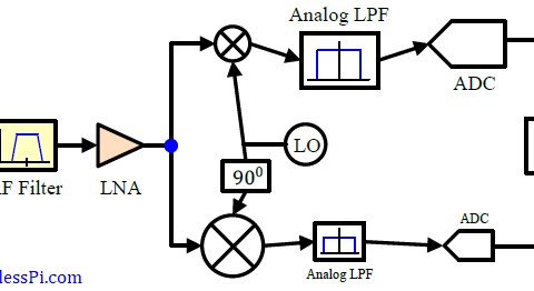
As drawn in the figure below, the first block in the Rx frontend is a Low Noise Amplifier (LNA). Next, the received signal is down-converted to a low intermediate frequency (IF). This combination of a variable IF along with variable band-pass filters provides flexibility with respect to channel selection at different channel spacings.
The band-pass filter frequency response follows a 2nd order Butterworth characteristic that provides adjacent channel signal attenuation before the analog to digital conversion. As opposed to the Tx frontend, the range from 160kHz to 2000kHz is covered with uniform logarithmic stepping.

Digital
As depicted in the above figure, the primary tasks accomplished by the Rx digital frontend are as follows.
- Sample rate conversion of the complex baseband signal
- Implementation of Automatic Gain Control (AGC) that maintains a predetermined signal amplitude at its output, despite variations in the signal amplitude at the input
- Estimation of Received Signal Strength Indicator (RSSI) that is a crude measure of received signal power
The ADC provides the raw data of the complex low-IF baseband signal at a sampling frequency of 32MHz. In the block DOWN_SRC(1:8), the raw data is downsampled to the sampling frequency of 4MHz and converted to zero-IF by the DOWN_MIX block. Depending on the configuration register RXDFE.SR, the signal is further down-sampled by the block DOWN\_SRC(1:SR) to the target receive sampling frequency given as
\[
f_s = \frac{4}{SR}~ \text{MHz}
\]
This is accomplished through a a linear phase FIR decimation filter with normalized cut-off frequency 1/SR. To deal with adjacent channel interference, the baseband signal can be further filtered by the block POST_FLT in which a selection of suitable normalized cut-off frequencies $f_{\text{cut}}$ is available. Here, you might also enjoy the description of Cascade Integrator Comb (CIC) filters and how they accomplish the task of sample rate conversion with minimal resources in digital frontends of transmitters and receivers.
Phase Measurement Unit (PMU)
For me, this is the most interesting feature of this device which is quite uncommon in any class of radio receivers. The Phase Measurement Unit (PMU) monitors and records the signal phase along with some other parameters at the output of the Rx frontend shown in the above figure. This is implemented at a constant PMU period of 8 $\mu$s.
In the above figure, let us denote the complex signal at the frontend output I_DATA and Q_DATA as
\[
x = x_i + jx_q
\]
Then, the datasheet shows the following expressions in the output registers.

This PMU unit has been widely used by the researchers in academia and industry for RF localization based on carrier phases. Finally, for applications requiring timing markers, each baseband core also contains a Timestamp Counter module with a 32-bit counter.
Conclusion
These AT86Rf215 transceivers were developed by ATMEL that was later acquired by Microchip. The product is quite useful for radio experimentation in communication and localization with a range of configurable blocks. Furthermore, the phase measurements provided by the PMU registers for external use are not a common offering in wireless industry. In my opinion, these transceivers fit quite well in the middle of the spectrum between hardware and software radios.
References
[1] Atmel AT86RF215 Datasheet: https://ww1.microchip.com/downloads/en/DeviceDoc/Atmel-42415-WIRELESS-AT86RF215_Datasheet.pdf