PLL design and analysis
From a functional perspective, a PLL is the most important block in a digital communication system and hence it requires careful mathematical understanding and design. Usually this is done through application of Laplace Transform in continuous-time case and z-Transform in discrete-time domain. However, for the sake of simplicity, we treat just one transform, namely the Discrete Fourier Transform (DFT) in our articles. Therefore, in regard to PLL design and analysis, we will take some key results from the literature without deriving them. This is due to our limitation of not covering the Laplace and z-Transforms. It should also be remembered that the design and analysis of a PLL does become mathematically untractable beyond an initial assumption of linearity and extensive computer simulations are needed in any case for its implementation in a particular application.
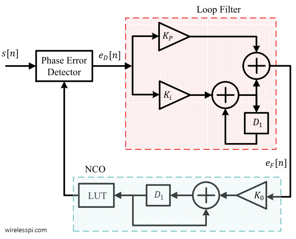
Let us start with a block diagram of a basic PLL shown in Figure below.
From a functional perspective, a PLL is the most important block in a digital communication system and hence it requires careful mathematical understanding and design. Usually this is done through application of Laplace Transform in continuous-time case and z-Transform in discrete-time domain. However, for the sake of simplicity, we treat just one transform, namely the Discrete Fourier Transform (DFT) in our articles. Therefore, in regard to PLL design and analysis, we will take some key results from the literature without deriving them. This is due to our limitation of not covering the Laplace and z-Transforms. It should also be remembered that the design and analysis of a PLL does become mathematically untractable beyond an initial assumption of linearity and extensive computer simulations are needed in any case for its implementation in a particular application.
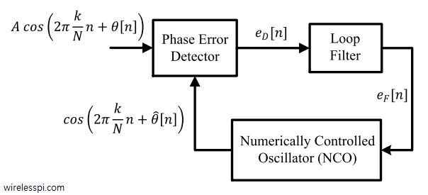 Assume that the discrete-time sinusoidal input to the PLL is given as
\begin{equation*}
\text{input} = A \cos \left( 2\pi \frac{k}{N}n + \theta[n]\right)
\end{equation*}
The PLL is designed in a way that the output is
\begin{equation*}
\text{output} = \cos \left( 2\pi \frac{k}{N}n + \hat\theta[n]\right)
\end{equation*}
where $\hat{\theta}[n]$ should be as close to $\theta[n]$ as possible after acquisition. This phase difference $\theta[n]-\hat\theta[n]$ is called phase error and is denoted by $\theta_e[n]$.
\begin{equation*}
\theta_e[n] = \theta[n] – \hat \theta[n]
\end{equation*}
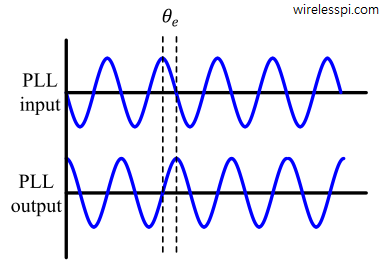
The phase error $\theta_e[n]$ computed at time $n$ is drawn in Figure below for a continuous-time signal.
Assume that the discrete-time sinusoidal input to the PLL is given as
\begin{equation*}
\text{input} = A \cos \left( 2\pi \frac{k}{N}n + \theta[n]\right)
\end{equation*}
The PLL is designed in a way that the output is
\begin{equation*}
\text{output} = \cos \left( 2\pi \frac{k}{N}n + \hat\theta[n]\right)
\end{equation*}
where $\hat{\theta}[n]$ should be as close to $\theta[n]$ as possible after acquisition. This phase difference $\theta[n]-\hat\theta[n]$ is called phase error and is denoted by $\theta_e[n]$.
\begin{equation*}
\theta_e[n] = \theta[n] – \hat \theta[n]
\end{equation*}
The phase error $\theta_e[n]$ computed at time $n$ is drawn in Figure below for a continuous-time signal.
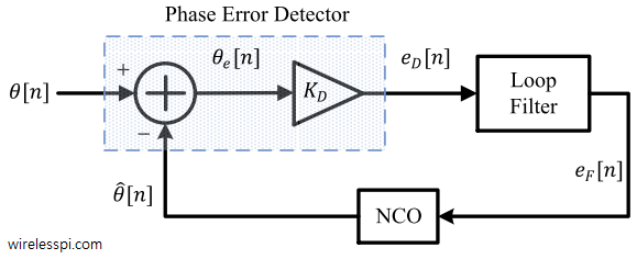
 The roles played by each block in the PLL are as follows.
[Phase error detector] A phase error detector determines the phase difference between a reference input waveform and a locally generated waveform and generates a corresponding signal denoted as $e_D[n]$.
[Loop filter] A loop filter sets the dynamic performance limits of a PLL. Moreover, it helps filter out noise and irrelevant frequency components generated in the phase error detector. Its output signal is denoted as $e_F[n]$.
[Numerically controlled oscillator (NCO)] An NCO generates a local discrete-time discrete-valued waveform with a phase as close to the phase of the reference signal as possible. The amount of the phase adjustment during each step is determined by the loop filter output.
As a first step towards our understanding, assume that $\theta[n]$ is zero and so the frequency of the input signal is $2\pi k/N$. Consequently,
The roles played by each block in the PLL are as follows.
[Phase error detector] A phase error detector determines the phase difference between a reference input waveform and a locally generated waveform and generates a corresponding signal denoted as $e_D[n]$.
[Loop filter] A loop filter sets the dynamic performance limits of a PLL. Moreover, it helps filter out noise and irrelevant frequency components generated in the phase error detector. Its output signal is denoted as $e_F[n]$.
[Numerically controlled oscillator (NCO)] An NCO generates a local discrete-time discrete-valued waveform with a phase as close to the phase of the reference signal as possible. The amount of the phase adjustment during each step is determined by the loop filter output.
As a first step towards our understanding, assume that $\theta[n]$ is zero and so the frequency of the input signal is $2\pi k/N$. Consequently,
- the NCO operates at the same frequency as well and the phase error $\theta_e$ is zero,
- then the phase error detector output $e_D[n]$ must ideally be zero,
- that leads to loop filter output $e_F[n]$ to be zero.
- the phase error detector would develop a non-zero output signal $e_D[n]$ which would rise or fall depending on $\theta_e$,
- the loop filter subsequently would generate a finite signal $e_F[n]$, and
- this would cause the NCO to change its phase in such a way as to turn $\theta_e$ towards zero again.
Phase error detector
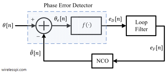
The phase error detector is a device which outputs some function $f\{\cdot\}$ of the difference between the phase $\theta[n]$ of the PLL input and the phase $\hat \theta[n]$ of the PLL output. So the phase error detector output is written as \begin{equation}\label{eqPLLPhaseDetectorOutput} e_D[n] = f \left\{\theta[n]-\hat \theta[n]\right\} = f\left\{\theta_e[n]\right\} \end{equation} The function $f\{\cdot\}$ is in general non-linear due to the fact that the phase $\theta[n]$ is embedded within the incoming sinusoid and is not directly accessible. A phase equivalent representation of such a PLL can be drawn by taking into account the phases of all sinusoids and tracking the operations on those phases through the loop. This is illustrated in Figure below.
 As mentioned before, a PLL is a non-linear device due to the phase error detector not having direct access to the sinusoidal phases. Although in reality the output is in general a non-linear function $f(\cdot)$ of the phase difference between the input and output sinusoids, a vast majority of the PLLs in locked condition can be approximated as linear due to the following reason.
In equilibrium, the loop has to keep adjusting the control signal $e_F[n]$ such that the output $\hat \theta[n]$ of the NCO is almost equal to the input phase $\theta[n]$. So during a proper operation, the phase error $\theta_e[n]$ should go to zero.
\begin{equation*}
\theta_e[n] = \theta[n] – \hat \theta[n] \rightarrow 0
\end{equation*}
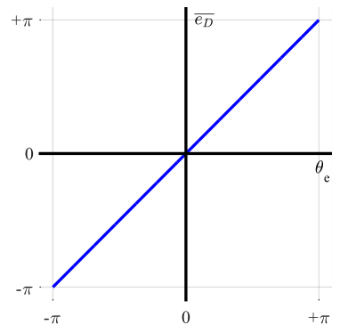
To make this happen, what should be the shape of the curve at the phase error detector output $e_D[n]=f(\theta_e[n])$?
For finding the answer, first assume that $\theta_e[n]$ is positive and see what can make it go to zero.
\begin{align*}
\theta_e[n] > 0 & \implies \theta[n] – \hat \theta[n] > 0 \\
& \implies \theta[n] > \hat \theta[n] \\
& \therefore ~~~~ \hat \theta [n]~ \text{should increase} \\
& \implies e_F[n]~ > 0 \\
& \implies e_D[n]~ > 0 \\
& \implies f(e[n]) > 0
\end{align*}
Similarly, when $\theta_e[n]<0$, it can be concluded that $e_D[n]=f(e[n])$ should be negative as well. This leads to the symbolic phase error detector input/output relationship drawn in Figure below for the phase error $\theta_e$ and average phase error detector output $\text{Mean}\{e_D[n]\}$ $\equiv$ $\overline{e_D}$. This kind of relationship is called an S-curve due to its shape resembling the English letter “S”. In articles on synchronization, we learn more about this shape and name.
As mentioned before, a PLL is a non-linear device due to the phase error detector not having direct access to the sinusoidal phases. Although in reality the output is in general a non-linear function $f(\cdot)$ of the phase difference between the input and output sinusoids, a vast majority of the PLLs in locked condition can be approximated as linear due to the following reason.
In equilibrium, the loop has to keep adjusting the control signal $e_F[n]$ such that the output $\hat \theta[n]$ of the NCO is almost equal to the input phase $\theta[n]$. So during a proper operation, the phase error $\theta_e[n]$ should go to zero.
\begin{equation*}
\theta_e[n] = \theta[n] – \hat \theta[n] \rightarrow 0
\end{equation*}
To make this happen, what should be the shape of the curve at the phase error detector output $e_D[n]=f(\theta_e[n])$?
For finding the answer, first assume that $\theta_e[n]$ is positive and see what can make it go to zero.
\begin{align*}
\theta_e[n] > 0 & \implies \theta[n] – \hat \theta[n] > 0 \\
& \implies \theta[n] > \hat \theta[n] \\
& \therefore ~~~~ \hat \theta [n]~ \text{should increase} \\
& \implies e_F[n]~ > 0 \\
& \implies e_D[n]~ > 0 \\
& \implies f(e[n]) > 0
\end{align*}
Similarly, when $\theta_e[n]<0$, it can be concluded that $e_D[n]=f(e[n])$ should be negative as well. This leads to the symbolic phase error detector input/output relationship drawn in Figure below for the phase error $\theta_e$ and average phase error detector output $\text{Mean}\{e_D[n]\}$ $\equiv$ $\overline{e_D}$. This kind of relationship is called an S-curve due to its shape resembling the English letter “S”. In articles on synchronization, we learn more about this shape and name.
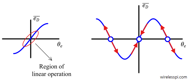 Under steady state conditions, $\theta_e[n]$ hovers around the origin and hence $e_D[n]=f(e[n])$ also stays within the region indicated with the red ellipse in Figure above. An extended typical S-curve is also drawn where one can observe that the PLL has the ability to pull back even a larger error $\theta_e[n]$. There is an increase in $e_D[n]$ with larger $\theta_e[n]$, thus $\hat \theta[n]$ increases and subsequently pulls $\theta_e[n] = \theta[n]-\hat\theta[n]$ back towards zero. However, the steering force depends on the magnitude of $e_D[n]$ which is different outside the linear region. It can be deduced that in the linear region of operation (a straight line relationship),
- a positive slope around zero produces a stable lock point, and
- a negative slope around zero does not generate a stable lock point.
 As we will find in other articles, the phase error detector is the most versatile block in a PLL that leads to an extremely wide range of PLL designs. On the other hand, depending on a certain application, there are set rules for choosing a loop filter and an NCO which simplify the process to some extent. In this article, our main purpose to employ PLLs is to build phase and timing synchronization modules instead of investigating the PLL theory in depth. Therefore, we will devise several different kinds of phase error detectors while using the same loop filter and NCO for each PLL.
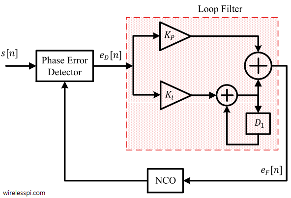
Proportional + Integrator (PI) Loop Filter
The loop filter in a PLL performs two main tasks.
- The primary task of a loop filter is to deliver a suitable control signal to the NCO and establish the dynamic performance of the loop. Most PLL applications require a loop filter that is capable of driving not only a phase offset between the input and output sinusoids to zero, but also tracking frequency offsets within a reasonable range. For larger carrier frequency offsets, a Frequency Locked Loop (FLL) is needed.
- A secondary task is to suppress the noise and high frequency signal components.
 For the sake of completion, it is important to know that
- a PLL without a loop filter (understandably known as a first order PLL) is also used in some applications where noise is not a primary concern [1], and
- a higher order loop filter can suppress spurs but increasing the order also increases the phase shift of such filters, thus making them prone to become unstable.
Numerically Controlled oscillator (NCO)
The signal $e_F[n]$ forms the input as a control signal to set the phase of an oscillator. The name controlled oscillator arises from the fact that its phase depends on the amplitude of the input control signal. Some examples of controlled oscillators are Voltage Controlled Oscillator (VCO) and a Numerically Controlled Oscillator (NCO). The oscillation frequency of a Voltage Controlled Oscillator (VCO) is controlled by its voltage input and hence it is an integral part of analog PLLs. As more and more functionality of the transceiver shifts towards the digital domain, the analog PLLs are seldom employed for waveform synchronization. A Numerically Controlled Oscillator (NCO) creates a discrete-time as well as discrete-valued (i.e., digital) representation of a waveform whose phase is steered by digital representation of a number at its input. In wireless communication devices, an NCO plays a central role in creating a digital version of a PLL for synchronization purpose and can even be used in analog modulation schemes like FM. It has two main components: [Phase Accumulator] The NCO adjusts its output phase $\hat{\theta}[n]$ based on its input signal $e_F[n]$ as \begin{equation*} \hat \theta[n] = K_0 \sum _{i=-\infty}^{n-1} e_F[i] \end{equation*} where $K_0$ is a constant of proportionality known as the oscillator gain. From this expression, we can see that an NCO acts as a phase accumulator. Note that the output can also be modified as \begin{align} \hat \theta[n] &= K_0 \sum _{i=-\infty}^{n-1} e_F[i] = K_0 \sum _{i=-\infty}^{n-2} e_F[i] + K_0\cdot e_F[n-1] \nonumber \\ &= \hat \theta[n-1] + K_0\cdot e_F[n-1] ~~~\text{mod}~ 2\pi \label{eqPLLControlledOscillator} \end{align} It can be deduced that an NCO executes backward difference integration to accumulate its input. Unlike the analog VCO, the gain $K_0$ of the phase accumulator can be easily set to a fixed value, say $1$, or some other normalizing factor. [Look-Up Table (LUT)] In embedded wireless devices, the phase update $\hat \theta[n]$ from the integrator serves as an index into a Look-Up Table (LUT) which stores the numeric values of a desired sampled waveform (such as a sine and a cosine). So the output can be computed as \begin{equation*} \begin{aligned} s_I[n]\: &= \cos \left( \hat \theta[n]\right)\\ s_Q[n] &= \sin \left( \hat \theta[n]\right) \end{aligned} \end{equation*} Naturally, the size of the lookup table determines the memory requirements as well as the amount of quantization on $\hat \theta[n]$, hence leading to a tradeoff between memory consumption and waveform approximation error. In most applications, a finer estimate is required to reduce this phase error noise which can be generated through interpolation between the stored samples, thus a change in the LUT size is not needed. With the inner workings of NCO available, a complete block diagram of a phase equivalent model of a PLL is now drawn in Figure below. The notation $D_1$ represents a delay of one sample time.
 As stated earlier, it is easier to establish the kind of loop filter and NCO according to the desired PLL performance and then search for a suitable phase error detector. For the purpose of carrier phase synchronization, we will continue to use a PI loop filter and an NCO for all different phase error detectors. For symbol timing synchronization, the loop filter will remain the same while a discrete-time interpolator will be employed instead of an NCO due to the nature of the underlying problem.
Designing a PLL
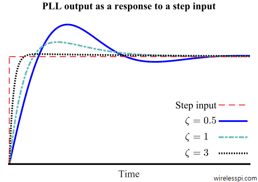
For the synchronization setup in this article, the PLL response is determined by two parameters: damping factor $\zeta$ and natural frequency $\omega_n$, which are taken from the standard control system terminology for a second order system. A description of $\zeta$ and $\omega_n$ is as follows. [Damping factor $\zeta$:] Imagine dropping a ball on the ground. After hitting the ground, the ball bounces up to a distance, and repeats damped oscillations before finally settling in equilibrium. Similarly, a PLL phase acquisition process exhibits an oscillatory behavior in the beginning which can be controlled by the damping factor. For a given input signal, a PLL behaves differently for different values of $\zeta$. This is illustrated in Figure below for a unit step phase input (when the input is a unit impulse, the output is an impulse response and when the input is a unit step, the output is known as a step response).
- When $\zeta < 1$, the loop response exhibits damped oscillations in the form of overshoots and undershoots and the system is termed as underdamped.
- When $\zeta > 1$, the loop response is the sum of decaying exponentials, oscillatory behaviour disappears with large $\zeta$ and the system is overdamped.
- Finally, when $\zeta = 1$, the response is somewhere between damped oscillations and decaying exponentials and the PLL is termed as critically damped.
 [Natural frequency $\omega_n$:] We will shortly see that the PLL in tracking mode acts as a lowpass filter. In this role, the natural frequency $\omega_n$ can be considered a coarse measure of the loop bandwidth.
PLL as a Lowpass Filter
The purpose of employing a PLL in a communications receiver is to track an incoming waveform in phase and frequency. This input signal is inherently corrupted by additive noise. In such a setup, a receiver locked in phase should reproduce this original signal adequately while removing as much noise as possible. The Rx uses a VCO or an NCO with a frequency close to that expected in the signal for this purpose. Through the loop filter, the PLL averages the phase error detector output over a length of time and keeps tuning its oscillator based on this average. If the input signal has a stable frequency, this long term average produces very accurate phase tracking, thus eliminating a significant amount of noise. In such a scenario, the input to the PLL is a noisy signal while the output is a clean version of the input. We can say that when operating as a linear tracking system, a PLL is a filter that passes signal and rejects noise.
Passband of a PLL
Having established the filtering operation of a PLL, we need to find out what kind of a filter a PLL is. For this purpose, consider the fact that within the linear region of operation, the PLL output phase closely follows the input phase for small and slow phase deviations. On the other hand, it loses lock for large and quick input variations, thus necessitating a lowpass frequency response.
Having established the filtering operation of a PLL, we need to find out what kind of a filter a PLL is. For this purpose, consider the fact that within the linear region of operation, the PLL output phase closely follows the input phase for small and slow phase deviations. On the other hand, it loses lock for large and quick input variations, thus necessitating a lowpass frequency response.
 The above figure shows the frequency response of a PLL with PI loop filter: it is indeed a lowpass filter. Before we think of it having a sharp transition bandwidth, remember that the frequency axis is also drawn on a logarithmic scale. Moreover, the frequency scale is normalized to natural frequency $\omega_n$ which makes the curve valid for all such PLLs.
The figure also reveals that the spectrum of this PLL as a lowpass filter is approximately flat between zero and $\omega_n$. This implies that the PLL should be able to track phase and frequency variations in the reference signal as long as these variations remain roughly below $\omega_n$.
By the same token, the bandwidth of this lowpass system varies with $\omega_n$. However, a better definition of the bandwidth is needed because the loop frequency response strongly depends on $\zeta$ for the same $\omega_n$. Therefore, a bandwidth measure known as the equivalent noise bandwidth $B_n$ (see Ref. [1]) is used that is related to natural frequency $\omega_n$ and damping factor $\zeta$ as
\begin{equation}\label{eqPLLBandwidth}
B_n = \frac{\omega_n}{2} \left( \zeta + \frac{1}{4\zeta}\right)
\end{equation}
for a PI loop filter.
The above figure shows the frequency response of a PLL with PI loop filter: it is indeed a lowpass filter. Before we think of it having a sharp transition bandwidth, remember that the frequency axis is also drawn on a logarithmic scale. Moreover, the frequency scale is normalized to natural frequency $\omega_n$ which makes the curve valid for all such PLLs.
The figure also reveals that the spectrum of this PLL as a lowpass filter is approximately flat between zero and $\omega_n$. This implies that the PLL should be able to track phase and frequency variations in the reference signal as long as these variations remain roughly below $\omega_n$.
By the same token, the bandwidth of this lowpass system varies with $\omega_n$. However, a better definition of the bandwidth is needed because the loop frequency response strongly depends on $\zeta$ for the same $\omega_n$. Therefore, a bandwidth measure known as the equivalent noise bandwidth $B_n$ (see Ref. [1]) is used that is related to natural frequency $\omega_n$ and damping factor $\zeta$ as
\begin{equation}\label{eqPLLBandwidth}
B_n = \frac{\omega_n}{2} \left( \zeta + \frac{1}{4\zeta}\right)
\end{equation}
for a PI loop filter.
Computing the Loop Constants
Designing a PLL in a software defined radio starts with defining the noise bandwidth $B_n$ and damping coefficient $\zeta$. [Loop noise bandwidth $B_n$:] As we will see in Example below, there is a tradeoff involved between choosing
- a small noise bandwidth that filters out most of the noise (and by extension the frequencies falling in the stopband), and
- a large noise bandwidth that can track fast phase variations, i.e., higher frequencies (and by extension allowing more noise to enter through the loop).
$$\begin{equation}
\begin{aligned}
K_P &\approx \frac {1}{K_DK_0L}\cdot \frac{4\zeta }{\zeta + \displaystyle\frac{1}{4\zeta}} \cdot \left(\frac{B_n}{R_M}\right)\\
&\\
K_i &\approx \frac{1}{K_DK_0L^2}\cdot \frac{4}{\left(\zeta + \displaystyle\frac{1}{4\zeta}\right)^2} \cdot \left(\frac{B_n}{R_M}\right)^2
\end{aligned}
\end{equation}\label{eqPLLLoopConstantsRM}$$
These are the equations we will use for computing the values for loop constants in specific PLL applications.
In summary, a software PLL whose code runs in a wireless device can be designed through the procedure outlined in Figure below.
 Next, we cover a few examples to demonstrate the phase tracking capability of a PLL and how different parameters influence its performance.
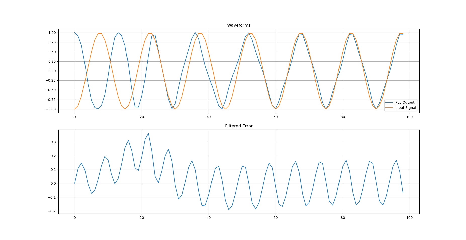
Example 1
Assume that the a PLL has to be designed such that it locks to a real sinusoid with discrete frequency $k/N = 1/15$ cycles/sample. Thus, the incoming sinusoid can be written as \begin{equation*} r[n] = A \cos \left( 2\pi \frac{1}{15} n + \theta[n]\right) \\ \end{equation*} where $\theta[n]$ can be a slowly changing phase. Here, we set a constant phase angle $\theta[n] = \pi$ that needs to be tracked. Such a large phase difference will enable us to clearly observe the PLL convergence process. The block diagram for such a system is drawn in Figure below. The NCO has one complex output, or two real outputs with an inphase and a quadrature component. \begin{equation*} \begin{aligned} s_I[n]\: &= \cos \left(2\pi\frac{k}{N}n + \hat \theta[n] \right) \\ s_Q[n] &= -\sin \left(2\pi\frac{k}{N}n + \hat \theta[n] \right) \end{aligned} \end{equation*}
The phase error detector is a simple multiplier that forms the product between the input sinusoid and the quadrature component of the NCO output. \begin{align*} e_D[n] &= -\sin \left(2\pi\frac{k}{N}n + \hat \theta[n] \right) \cdot A \cos \left( 2\pi \frac kN n + \theta[n]\right) \\ &= \frac A2 \sin \Big( \theta[n] – \hat \theta[n]\Big) – \frac A2 \sin \left(2\pi \frac {2\cdot k}{N} n + \theta[n] + \hat \theta[n] \right) \\ &= \frac A2 \sin \Big( \theta_e[n]\Big) + \text{double frequency term} \end{align*} where the identity $\cos(A)\sin(B)$ $= \frac{1}{2}$ $\left\{ \sin(A+B)\right.\}$ $-$ $\left.\sin(A-B) \right\}$ has been used. The second term involving $2\pi (2\cdot k/N)$ is the double frequency term that is filtered out by the loop filter. Therefore, the loop tracks the first term only, given by \begin{equation*} e_D[n] \approx \frac A2 \sin \Big( \theta_e[n] \Big) \end{equation*} The S-curve is the sine of $\theta_e$ which can be approximated using the identity $\sin A \approx A$ for small $A$. For this reason, the phase error detector output is approximately linear for steady state operation around the origin. \begin{align*} \overline{e_D} &= \frac A2 \sin \theta_e \\ &\approx \frac A2 \theta_e \quad \text{for small}~\theta_e \end{align*} This S-curve is plotted in Figure below.
From the above equation, the phase error detector gain $K_D$ is clearly seen to be \begin{equation*} K_D = \frac A2 \end{equation*} and hence is a function of sinusoid amplitude at the PLL input. Remember from Eq (\ref{eqPLLLoopConstantsFS}) that loop filter gains $K_P$ and $K_i$ involve $K_D$ in their expressions. If the input signal level is not controlled, loop filter will have incorrect coefficients and the design will not perform as expected. In a wireless receiver, this amplitude is maintained at a predetermined value by using an Automatic Gain Control (AGC). For the purpose of this example, we assume that $A$ is fixed to $1$ and hence \begin{equation*} K_D=0.5 \end{equation*} Next, we design a PLL with damping factor \begin{equation*} \zeta = 1/\sqrt{2} = 0.707 \end{equation*} and loop noise bandwidth $B_n = 5\%$ of the sample rate $F_S$, or \begin{equation*} B_n/F_S = 0.05 \end{equation*} Thus, plugging these parameters in Eq (\ref{eqPLLLoopConstantsFS}), we get \begin{align*} K_P &= 0.2667 \\ K_i &= 0.0178 \end{align*} After setting the rest of the parameters at the start of this example, the PLL can be simulated through any programming loop in a software routine that computes the sample-by-sample product of the loop input and quadrature loop output.
Assume that the a PLL has to be designed such that it locks to a real sinusoid with discrete frequency $k/N = 1/15$ cycles/sample. Thus, the incoming sinusoid can be written as \begin{equation*} r[n] = A \cos \left( 2\pi \frac{1}{15} n + \theta[n]\right) \\ \end{equation*} where $\theta[n]$ can be a slowly changing phase. Here, we set a constant phase angle $\theta[n] = \pi$ that needs to be tracked. Such a large phase difference will enable us to clearly observe the PLL convergence process. The block diagram for such a system is drawn in Figure below. The NCO has one complex output, or two real outputs with an inphase and a quadrature component. \begin{equation*} \begin{aligned} s_I[n]\: &= \cos \left(2\pi\frac{k}{N}n + \hat \theta[n] \right) \\ s_Q[n] &= -\sin \left(2\pi\frac{k}{N}n + \hat \theta[n] \right) \end{aligned} \end{equation*}

Phase Error Detector
The phase error detector is a simple multiplier that forms the product between the input sinusoid and the quadrature component of the NCO output. \begin{align*} e_D[n] &= -\sin \left(2\pi\frac{k}{N}n + \hat \theta[n] \right) \cdot A \cos \left( 2\pi \frac kN n + \theta[n]\right) \\ &= \frac A2 \sin \Big( \theta[n] – \hat \theta[n]\Big) – \frac A2 \sin \left(2\pi \frac {2\cdot k}{N} n + \theta[n] + \hat \theta[n] \right) \\ &= \frac A2 \sin \Big( \theta_e[n]\Big) + \text{double frequency term} \end{align*} where the identity $\cos(A)\sin(B)$ $= \frac{1}{2}$ $\left\{ \sin(A+B)\right.\}$ $-$ $\left.\sin(A-B) \right\}$ has been used. The second term involving $2\pi (2\cdot k/N)$ is the double frequency term that is filtered out by the loop filter. Therefore, the loop tracks the first term only, given by \begin{equation*} e_D[n] \approx \frac A2 \sin \Big( \theta_e[n] \Big) \end{equation*} The S-curve is the sine of $\theta_e$ which can be approximated using the identity $\sin A \approx A$ for small $A$. For this reason, the phase error detector output is approximately linear for steady state operation around the origin. \begin{align*} \overline{e_D} &= \frac A2 \sin \theta_e \\ &\approx \frac A2 \theta_e \quad \text{for small}~\theta_e \end{align*} This S-curve is plotted in Figure below.

Loop Constants
From the above equation, the phase error detector gain $K_D$ is clearly seen to be \begin{equation*} K_D = \frac A2 \end{equation*} and hence is a function of sinusoid amplitude at the PLL input. Remember from Eq (\ref{eqPLLLoopConstantsFS}) that loop filter gains $K_P$ and $K_i$ involve $K_D$ in their expressions. If the input signal level is not controlled, loop filter will have incorrect coefficients and the design will not perform as expected. In a wireless receiver, this amplitude is maintained at a predetermined value by using an Automatic Gain Control (AGC). For the purpose of this example, we assume that $A$ is fixed to $1$ and hence \begin{equation*} K_D=0.5 \end{equation*} Next, we design a PLL with damping factor \begin{equation*} \zeta = 1/\sqrt{2} = 0.707 \end{equation*} and loop noise bandwidth $B_n = 5\%$ of the sample rate $F_S$, or \begin{equation*} B_n/F_S = 0.05 \end{equation*} Thus, plugging these parameters in Eq (\ref{eqPLLLoopConstantsFS}), we get \begin{align*} K_P &= 0.2667 \\ K_i &= 0.0178 \end{align*} After setting the rest of the parameters at the start of this example, the PLL can be simulated through any programming loop in a software routine that computes the sample-by-sample product of the loop input and quadrature loop output.
Phase Error Detector Output $e_D[n]$
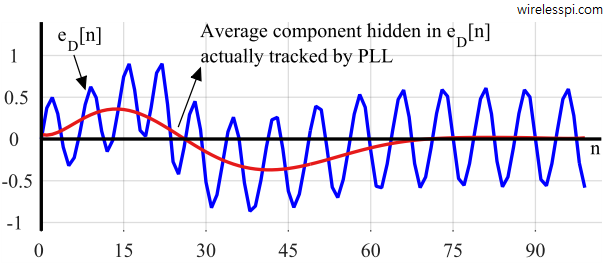
We start with the plot shown in Figure below displaying $e_D[n]$ that contains the following two components.
- A slowly varying average component hidden in $e_D[n]$ is shown in red. This can be thought of the true phase error to which the loop responds by converging to the incoming phase. Observe that this error stays positive for the first $27$ samples, then goes negative before settling to zero at around $70$ samples mark. Therefore, as we will see later, the NCO output should overcome the initial phase difference of $\pi$ and track the input sinusoid after around $70$ samples.
- A constant amplitude sinusoid with double frequency $2 \cdot 2\pi (k/N)$ $=$ $2\pi (2/15)$. Observe in Figure that every $15$ samples, there are $2$ complete oscillations of this sinusoid riding on average error curve. This is more clearly visible towards the end of the curve where steady state is seen to be reached. Since $A/2=0.5$, the amplitude of this double frequency term approximately varies from around $-0.5$ to $+0.5$, resulting in a peak-to-peak amplitude of $1$.
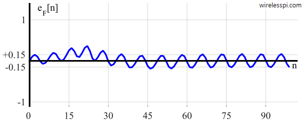
Loop Filter Output $e_F[n]$
Figure below displays the error signal $e_F[n]$ at the output of the loop filter. Similar kinds of trajectories are visible as in $e_D[n]$. However, the amplitude of double frequency term has been reduced from a peak-to-peak value of $1$ in $e_D[n]$ to a peak-to-peak value of $0.3$. This behaviour reinforces the lowpass characteristic of a PLL. Recall that the input sinusoid has a discrete frequency $k/N=1/15$ which was chosen for the purpose of better visualization of error convergence. If we had chosen a higher frequency, the attenuation of double frequency term would have been different.
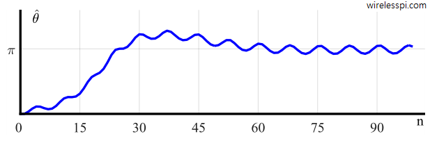
Phase Estimate $\hat \theta[n]$
The phase estimate $\hat \theta[n]$ is plotted in Figure below. Just like $e_D[n]$ approaching zero after $70$ samples, $\hat \theta[n]$ is seen to approach the initial phase difference $\pi$ between the input and PLL output sinusoids. The oscillations due to double frequency term still remain. Observe that the phase estimate does not directly converge to the actual value of $\pi$. Instead, its average value exhibits oscillatory behaviour by going beyond $\pi$, then returning and oscillating around this value, which could have been clearer if the figure was extended to display more samples. This is due to the value chosen for the damping factor $\zeta = 0.707$. Just like dropping a ball on the ground, the phase estimate $\hat \theta[n]$ repeats damped oscillations before finally settling at the equilibrium.
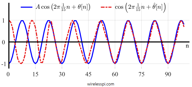
PLL Output Sinusoid
Finally, the output inphase sinusoid $\cos \left( 2\pi (k/N) n + \hat \theta[n]\right)$ is shown along with the input sinusoid in Figure below. Initially, there is a phase difference of $\pi$ between them but gradually the PLL compensates for this difference and approaches the input sinusoid tracking successfully afterwards. This happens after $70$ samples where $e_D[n]$ was seen to draw towards zero. Interestingly, the little oscillatory behaviour shown by $\hat \theta[n]$ can be spotted here as well after convergence has reached, where the red dashed curve slightly leads and then slightly lags behind the input blue curve.
Python code for a Phase Locked Loop (PLL)
# PLL in an SDR

# Import the necessary packages and modules
import matplotlib.pyplot as plt
import numpy as np

k = 1
N = 15
K_p = 0.2667
K_i = 0.0178
K_0 = 1

input_signal = np.zeros(100)

integrator_out = 0
phase_estimate = np.zeros(100)
e_D = [] #phase-error output
e_F = [] #loop filter output
sin_out = np.zeros(100)
cos_out = np.ones(100)

for n in range(99):
    input_signal[n] = np.cos(2*np.pi*(k/N)*n + np.pi)

    # phase detector
    try:
        e_D.append(input_signal[n] * sin_out[n])
    except IndexError:
        e_D.append(0)


    #loop filter
    integrator_out += K_i * e_D[n]
    e_F.append(K_p * e_D[n] + integrator_out)


    #NCO
    try:
        phase_estimate[n+1] = phase_estimate[n] + K_0 * e_F[n]
    except IndexError:
        phase_estimate[n+1] = K_0 * e_F[n]

    sin_out[n+1] = -np.sin(2*np.pi*(k/N)*(n+1) + phase_estimate[n])
    cos_out[n+1] = np.cos(2*np.pi*(k/N)*(n+1) + phase_estimate[n])


# Create a Figure
fig = plt.figure()

# Set up Axes
ax1 = fig.add_subplot(211)
ax1.plot(cos_out, label='PLL Output')
plt.grid()
ax1.plot(input_signal, label='Input Signal')
plt.legend()
ax1.set_title('Waveforms')

# Show the plot
#plt.show()

ax2 = fig.add_subplot(212)
ax2.plot(e_F)
plt.grid()
ax2.set_title('Filtered Error')
plt.show()
 Similar to the above example, different PLLs can be designed for different phase detectors, different values of damping factor $\zeta$ and loop noise bandwidth $B_n$ and the results can be plotted to see how each parameter value affects the PLL behaviour. In the next example, we implement a PLL based on complex signal processing.
Example 2
The PLL now has to be designed such that it locks to a complex sinusoid with discrete frequency $k/N = 1/15$ cycles/sample. Thus, the input sinusoid can be written as \begin{equation*} \begin{aligned} r_I[n]\: &= A\cos \left(2\pi\frac{k}{N}n + \theta[n] \right) \\ r_Q[n] &= A\sin \left(2\pi\frac{k}{N}n + \theta[n] \right) \end{aligned} \end{equation*} The block diagram for such a system is drawn in Figure below. The NCO also has a complex output, or two real outputs with an inphase and a quadrature component, written as \begin{equation*} \begin{aligned} s_I[n]\: &= \cos \left(2\pi\frac{k}{N}n + \hat \theta[n] \right) \\ s_Q[n] &= -\sin \left(2\pi\frac{k}{N}n + \hat \theta[n] \right) \end{aligned} \end{equation*}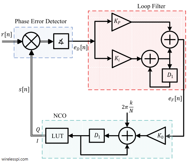 Here, the phase detector first computes the product of the input and output complex sinusoids. Although the block diagram shows a simple product operator, remember that a complex product actually implements $4$ real multiplications and $2$ real additions. Using the trigonometric identities as before, the double frequency terms simply cancel out and the result of the product is
\begin{equation*}
\begin{aligned}
\{r[n]\cdot s[n]\}_I\: &= \cos \left(\hat \theta[n] – \hat \theta[n] \right) = \cos \theta_e[n] \\
\{r[n]\cdot s[n]\}_Q &= \sin \left( \hat \theta[n] – \hat \theta[n] \right) = \sin \theta_e[n]
\end{aligned}
\end{equation*}
Note the difference in complex signal processing: the double frequency terms actually cancel out instead of being filtered out by the loop filter. Furthermore, the phase of the above complex signal is precisely the error signal which needs to be extracted to form $e_D[n]$.
Accordingly, a four-quadrant inverse tangent defined in the article on complex numbers is used to compute the phase of this complex signal at multiplier output. Therefore, the output of the phase detector is simply
\begin{equation*}
e_D[n] = \measuredangle \big(r[n]\cdot s[n]\big) = \theta_e[n]
\end{equation*}
for which the corresponding S-curve is drawn in Figure below.
\begin{equation*}
\overline{e_D} = \theta_e
\end{equation*}
Notice that the S-curve is linear over the whole range $-\pi \le \theta_e \le \pi$ and its expression implies that the phase detector gain $K_D$ $=1$.
Here, the phase detector first computes the product of the input and output complex sinusoids. Although the block diagram shows a simple product operator, remember that a complex product actually implements $4$ real multiplications and $2$ real additions. Using the trigonometric identities as before, the double frequency terms simply cancel out and the result of the product is
\begin{equation*}
\begin{aligned}
\{r[n]\cdot s[n]\}_I\: &= \cos \left(\hat \theta[n] – \hat \theta[n] \right) = \cos \theta_e[n] \\
\{r[n]\cdot s[n]\}_Q &= \sin \left( \hat \theta[n] – \hat \theta[n] \right) = \sin \theta_e[n]
\end{aligned}
\end{equation*}
Note the difference in complex signal processing: the double frequency terms actually cancel out instead of being filtered out by the loop filter. Furthermore, the phase of the above complex signal is precisely the error signal which needs to be extracted to form $e_D[n]$.
Accordingly, a four-quadrant inverse tangent defined in the article on complex numbers is used to compute the phase of this complex signal at multiplier output. Therefore, the output of the phase detector is simply
\begin{equation*}
e_D[n] = \measuredangle \big(r[n]\cdot s[n]\big) = \theta_e[n]
\end{equation*}
for which the corresponding S-curve is drawn in Figure below.
\begin{equation*}
\overline{e_D} = \theta_e
\end{equation*}
Notice that the S-curve is linear over the whole range $-\pi \le \theta_e \le \pi$ and its expression implies that the phase detector gain $K_D$ $=1$.
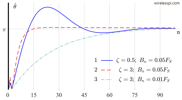
 Now we design three PLLs with different damping factors $\zeta$ and loop noise bandwidth normalized with sample rate $B_n/F_S$ as follows.
[Case 1] $\zeta = 1/2$ and $B_n/F_S = 0.05$
[Case 2] $\zeta = 3$ and $B_n/F_S = 0.05$
[Case 3] $\zeta = 3$ and $B_n/F_S = 0.01$
Loop filter coefficients $K_P$ and $K_i$ can be found by plugging these values in Eq (\ref{eqPLLLoopConstantsFS}). Next, the PLL can be simulated as in the previous example and the phase detector output $e_D[n]$ as well as the phase estimate $\hat \theta[n]$ are plotted for these three PLLs in Figures below.
Now we design three PLLs with different damping factors $\zeta$ and loop noise bandwidth normalized with sample rate $B_n/F_S$ as follows.
[Case 1] $\zeta = 1/2$ and $B_n/F_S = 0.05$
[Case 2] $\zeta = 3$ and $B_n/F_S = 0.05$
[Case 3] $\zeta = 3$ and $B_n/F_S = 0.01$
Loop filter coefficients $K_P$ and $K_i$ can be found by plugging these values in Eq (\ref{eqPLLLoopConstantsFS}). Next, the PLL can be simulated as in the previous example and the phase detector output $e_D[n]$ as well as the phase estimate $\hat \theta[n]$ are plotted for these three PLLs in Figures below.
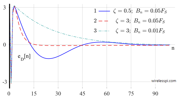
Here, some comments about acquisition and locking behaviour of a PLL are in order.
The PLL now has to be designed such that it locks to a complex sinusoid with discrete frequency $k/N = 1/15$ cycles/sample. Thus, the input sinusoid can be written as \begin{equation*} \begin{aligned} r_I[n]\: &= A\cos \left(2\pi\frac{k}{N}n + \theta[n] \right) \\ r_Q[n] &= A\sin \left(2\pi\frac{k}{N}n + \theta[n] \right) \end{aligned} \end{equation*} The block diagram for such a system is drawn in Figure below. The NCO also has a complex output, or two real outputs with an inphase and a quadrature component, written as \begin{equation*} \begin{aligned} s_I[n]\: &= \cos \left(2\pi\frac{k}{N}n + \hat \theta[n] \right) \\ s_Q[n] &= -\sin \left(2\pi\frac{k}{N}n + \hat \theta[n] \right) \end{aligned} \end{equation*}
 Here, the phase detector first computes the product of the input and output complex sinusoids. Although the block diagram shows a simple product operator, remember that a complex product actually implements $4$ real multiplications and $2$ real additions. Using the trigonometric identities as before, the double frequency terms simply cancel out and the result of the product is
\begin{equation*}
\begin{aligned}
\{r[n]\cdot s[n]\}_I\: &= \cos \left(\hat \theta[n] – \hat \theta[n] \right) = \cos \theta_e[n] \\
\{r[n]\cdot s[n]\}_Q &= \sin \left( \hat \theta[n] – \hat \theta[n] \right) = \sin \theta_e[n]
\end{aligned}
\end{equation*}
Note the difference in complex signal processing: the double frequency terms actually cancel out instead of being filtered out by the loop filter. Furthermore, the phase of the above complex signal is precisely the error signal which needs to be extracted to form $e_D[n]$.
Accordingly, a four-quadrant inverse tangent defined in the article on complex numbers is used to compute the phase of this complex signal at multiplier output. Therefore, the output of the phase detector is simply
\begin{equation*}
e_D[n] = \measuredangle \big(r[n]\cdot s[n]\big) = \theta_e[n]
\end{equation*}
for which the corresponding S-curve is drawn in Figure below.
\begin{equation*}
\overline{e_D} = \theta_e
\end{equation*}
Notice that the S-curve is linear over the whole range $-\pi \le \theta_e \le \pi$ and its expression implies that the phase detector gain $K_D$ $=1$.
Here, the phase detector first computes the product of the input and output complex sinusoids. Although the block diagram shows a simple product operator, remember that a complex product actually implements $4$ real multiplications and $2$ real additions. Using the trigonometric identities as before, the double frequency terms simply cancel out and the result of the product is
\begin{equation*}
\begin{aligned}
\{r[n]\cdot s[n]\}_I\: &= \cos \left(\hat \theta[n] – \hat \theta[n] \right) = \cos \theta_e[n] \\
\{r[n]\cdot s[n]\}_Q &= \sin \left( \hat \theta[n] – \hat \theta[n] \right) = \sin \theta_e[n]
\end{aligned}
\end{equation*}
Note the difference in complex signal processing: the double frequency terms actually cancel out instead of being filtered out by the loop filter. Furthermore, the phase of the above complex signal is precisely the error signal which needs to be extracted to form $e_D[n]$.
Accordingly, a four-quadrant inverse tangent defined in the article on complex numbers is used to compute the phase of this complex signal at multiplier output. Therefore, the output of the phase detector is simply
\begin{equation*}
e_D[n] = \measuredangle \big(r[n]\cdot s[n]\big) = \theta_e[n]
\end{equation*}
for which the corresponding S-curve is drawn in Figure below.
\begin{equation*}
\overline{e_D} = \theta_e
\end{equation*}
Notice that the S-curve is linear over the whole range $-\pi \le \theta_e \le \pi$ and its expression implies that the phase detector gain $K_D$ $=1$.
 Now we design three PLLs with different damping factors $\zeta$ and loop noise bandwidth normalized with sample rate $B_n/F_S$ as follows.
[Case 1] $\zeta = 1/2$ and $B_n/F_S = 0.05$
[Case 2] $\zeta = 3$ and $B_n/F_S = 0.05$
[Case 3] $\zeta = 3$ and $B_n/F_S = 0.01$
Loop filter coefficients $K_P$ and $K_i$ can be found by plugging these values in Eq (\ref{eqPLLLoopConstantsFS}). Next, the PLL can be simulated as in the previous example and the phase detector output $e_D[n]$ as well as the phase estimate $\hat \theta[n]$ are plotted for these three PLLs in Figures below.
Now we design three PLLs with different damping factors $\zeta$ and loop noise bandwidth normalized with sample rate $B_n/F_S$ as follows.
[Case 1] $\zeta = 1/2$ and $B_n/F_S = 0.05$
[Case 2] $\zeta = 3$ and $B_n/F_S = 0.05$
[Case 3] $\zeta = 3$ and $B_n/F_S = 0.01$
Loop filter coefficients $K_P$ and $K_i$ can be found by plugging these values in Eq (\ref{eqPLLLoopConstantsFS}). Next, the PLL can be simulated as in the previous example and the phase detector output $e_D[n]$ as well as the phase estimate $\hat \theta[n]$ are plotted for these three PLLs in Figures below.


Comments on Locking and Acquisition
A complete study of a PLL design and performance involves an in-depth mathematical formulation including solutions to non-linear equations. Just like we took some key results for PLL design without deriving them, we next comment on some key parameters that govern its performance. We start with the parameters that specify the frequency range within which a PLL can be operated. The details of most of what follows are nicely explained in Ref. [1].
Hold range
There is a critical value of the frequency offset between the input and output waveforms after which the slightest disturbance causes the PLL to lose phase tracking forever. This range, in which a PLL can statically maintain phase tracking, is known as hold range $F_H$.
Pull-in range
When the frequency offset of the reference signal in an unlocked state reduces below another critical value, the buildup of the average phase error starts decelerating thus leading to an eventual system lock. This value is known as pull-in range $F_P$. The pull-in range is significantly smaller than the hold range. Even though the pull-in process itself is relatively slow, the PLL will always become locked for an offset within this range.
Lock range
Obtaining a locked state within a short time duration is desirable in most applications. If the frequency offset reduces below another value — called the lock range $F_L$– the PLL becomes locked within one single-beat note between the reference and the output frequencies. The lock range is much smaller than the pull-in range; however on the up side, the lock-in process itself is much faster than the pull-in process. Remember that the lock actually implies that for each cycle of the input, there is one and only one cycle of NCO output. Even with a phase lock, both steady phase errors and fluctuating phase errors can be present. In practical applications, the operating frequency range of a PLL is normally restricted to the lock range. In summary, the hold range and the lock range are the largest and the smallest, respectively, while the pull-in range lies somewhere within the boundaries set by them. Thus, the following inequality holds. \begin{equation*} F_H > F_P > F_L \end{equation*} Next, we describe two other important quantities which determine the suitability of a PLL for an application.
Acquisition time
A PLL requires a finite amount of time to successfully adjust to the incoming signal and reduce the phase error to zero, which is called acquisition time. The acquisition time is given by the sum of the time to achieve frequency lock as well as that of the phase lock. It is inversely proportional to $B_n$ because a PLL with a large noise bandwidth lets more frequencies through its passband, consequently becoming able to track rapid variations and locking quicker than a PLL with narrower noise bandwidth. In above Figures, this can be noticed in a comparison between cases $2$ and $3$ with same $\zeta=3$ but different loop noise bandwidths. As a general rule, for a frequency offset $F_\Delta$, \begin{equation}\label{eqPLLAcquisitionTime} T_{\text{acq}} \propto \frac{F_\Delta^2}{B_n^3} \end{equation}
Tracking error
The performance of a PLL is determined by tracking error which is the power of the phase error signal. For a PLL in tracking mode (i.e., during linear operation), the noise power at the PLL input is given by AWGN with power spectral density $N_0$ defined in article on AWGN and the loop noise bandwidth $B_n$ as \begin{equation*} P_w = N_0 \cdot B_n \end{equation*} For a sinusoidal input with power $P_s$ at the PLL input, the ratio $P_s/P_w$ is the Signal-to-Noise Ratio (SNR). The expression for the tracking error $\rho_{\theta_e}$ is \begin{equation}\label{eqPLLTrackingError} \rho_{\theta_e} = \frac{N_0 B_n}{P_s} = \frac{P_w}{P_s} = \frac{1}{P_s/P_w} \end{equation} Therefore, the tracking error in the presence of AWGN is inversely proportional to SNR and consequently directly proportional to $B_n$. It makes sense that a wider bandwidth allows a larger amount of noise at the PLL output, thus increasing the tracking error.
This PLL Does Not Work in an Actual Modem!
Interestingly, all the details we have worked out about a PLL do not make it work in an actual digital communication system. This is due to the fundamental problem of synchronization according to which a PLL cannot lock onto a carrier wave changing its phase and amplitude at symbol rate. Therefore, an actual implementation goes through the following two steps.
- Modify the error detector such that it wipes off the modulation.
- Apply the PLL principles to this (now unmodulated) waveform.
A Fast Lock Technique
From Eq (\ref{eqPLLAcquisitionTime}) above, it is evident that selecting a large $B_n$ in PLL design results in faster acquisition since the acquisition time is inversely proportional to a power of $B_n$. On the other hand, Eq (\ref{eqPLLTrackingError}) shows that a narrow $B_n$ generates less tracking error since it is directly proportional to $B_n$. In conclusion, a good PLL design balances the opposite criteria of fast acquisition time and reduced tracking error. In the world of hardware radio, PLL designers had to balance these two performance criteria by finding an acceptable compromise. The realm of software radio offers a better solution due to our ability to change the code on the fly which is explained below. In an unlocked state, the PLL noise bandwidth $B_n$ is made large so that it can achieve fast lock. In parallel, a certain algorithm known as a lock detector is run which generates a binary output depending on whether the PLL has acquired lock or not. Since the loop constants are reconfigurable in this scenario, their values are changed such that the PLL bandwidth $B_n$ is reduced to a smaller value. In other articles, we discuss carrier and timing synchronization procedures in a communications receiver. These blocks incorporate a PLL as an integral component. We also introduce some of the issues faced during a practical implementation. Finally, a Kalman filter can be incorporated in any synchronization system for improved performance.
References
[1] R. Best, Phase Locked Loops – Design, Simulation and Applications (6th Edition), McGraw Hill, 2007. [2] M. Rice, Digital Communications – A Discrete-Time Approach, Prentice Hall, 2009.
Awesome post. Great!
Glad you liked it.
I’ve scoured google and this is the only resource I could find that got me to the point of feeling I could implement an SPLL on my own. Most others threw giant equations at me in the 2nd sentence that made me feel like I was sleeping in EE academic lectures.
Well done!
My application for SPLL is a very low frequency input signal with a lot of amplitude variation. I’m not yet sure if AGC will need to be so extreme that it will impart error in my signal.
Alternatively would it be practical for K values to be tweaked in realtime in response to changes in my input signal amplitude?
Both options, an AGC or varying loop filter coefficients, can be implemented. However, if the signal amplitude variations are fast enough to impact the PLL performance, the AGC option is preferred as compared to tweaking K values.
I have a question regarding the basic operation of a CDR. Why don’t we make the loop bandwidth of a CDR as large as possible? Suppose we can make the bandwidth arbitrarily wide, then the CDR should be able to track out any jitter of the incoming data, or maybe we can say the recovered clock is now “perfectly synced” to the incoming data. Although the recovered clock itself is not clean, on the other hand, we won’t “see” any jitter of the incoming data as well. Is this right?
A large loop bandwidth allows high noise power to enter the system and affect the loop performance. The best way is to start with a large loop bandwidth but reduce it step by step while passing through acquisition to tracking mode.
Thank you for your reply! I can understand your suggestion but I’m still in doubt regarding the loop bandwidth. If I’m only interested in using the recovered clock to retime the data. Then in theory an arbitrarily large loop bandwidth will push the corner frequency of the OJTF way above the highest jitter frequency, so that I won’t observe any jitter in the data.
Such a great article, thank you posting.
I have a question: What particular SDRs have the option to reconfigure its PLL on the fly? Because the SDRs that I happen to work with (Ettus and NI USRPs) do not seem to have this option.
There are different types of PLLs in a radio system (e.g., used in frequency synthesizers, timing and carrier synchronization, etc.). The PLL we are talking about is a software based carrier phase synchronizer which works in a piece of code written by the designer. So SDRs have this option to reconfigure these PLLs on the fly.
A very complicated device is explained in a simple way. Great job done.
Thank you.
Hi, thanks a lot for your article. Could you please clarify, if the loop_bw in control_loop.cc (gr-analog) is the natural frequency omega_n or the equivalent noise bandwidth B_n in your article ? I’m a beginner trying to understand how the gr pll work so as to be able to fine tune it. Cheers!
It is the natural frequency omega_n, not the equivalent noise bandwidth B_n.
A confusion on the statement “a large ζ results in no overshoots but long convergence time while a small ζ exhibits relatively fast convergence but damped oscillations.”
Actually if we look at the figure https://wirelesspi.com/wp-content/uploads/2017/08/figure-pll-step-response.png, it seems small ζ converges slowly than large ζ (due to damping). Am I understanding wrong?
Hi Hao. If we could look at the figure beyond the drawn time, large $\zeta$ takes a longer time to converge.
In equation 3, is $B_n$ in Hz or rad/sec? When $B_n/F_s$ = 0.05, does that mean if $F_s$ = 100 Hz, $B_n$ = 5 Hz or 5 rad/sec? I think this affects the computed loop constants, like there’s a missing conversion factor from Hz to rad/sec or vice versa.
The equivalent noise bandwidth $B_n$ is in Hz here. And yes, including a conversion factor would affect the results.
Noted. Nice article, makes me appreciate PLL more since building the software version is more accessible. Thanks!
Very cool article! I am going to implement a software-based phase-locked loop to stabilize (derotate) the constellation display on my signal analyzer app. Thank’s much!
That’s good to know. Just keep in mind that for implementing a PLL at the demodulator, you need to go one step above this tutorial (as it covers a basic PLL without modulation). Chapter 5 of my wireless communications book might prove useful for this purpose.
The only useful resource on internet to understand SWPLL the layman way!. Great Job!